


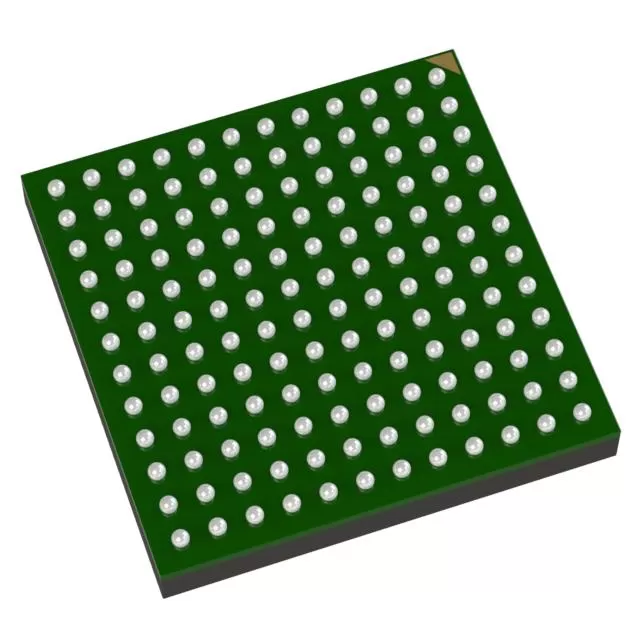

LT3757AEMSE#TRPBF
Brand: Analog Devices
Analog Devices LT3757AEMSE#TRPBF is a analog & mixed-signal component designed for Precision Instrumentation and related applications. In stock at Superb Automation — request a quote for competitive pricing and fast delivery.
Product Specifications
LT3757AEMSE#TRPBF
Analog Devices — Analog & Mixed-Signal ICs
Product Overview
The LT3757AEMSE#TRPBF from Analog Devices is a high-performance analog / mixed-signal IC providing precision signal acquisition, conversion, and conditioning. Analog Devices (ADI) is a world leader in high-performance analog, mixed-signal, and DSP ICs for instrumentation, healthcare, automotive, and communications.
Superb Automation partners with leading brands including Qorvo, TI, ADI, XILINX, NVIDIA, Intel, ST, MACOM, Renesas, and Coilcraft to provide complete BOM and supply-chain solutions.
Key Features
- High-resolution data conversion with excellent SNR and THD
- Wide dynamic range and high linearity across operating conditions
- Integrated voltage reference with low temperature drift
- Flexible digital interface — SPI, I2C, or parallel options
- Industrial/automotive temperature range with guaranteed specs
- Low power consumption with power-down modes
Key Specifications
| Resolution | bits |
| Channels | — |
| Sample Rate | kSPS |
| Interface | — |
| Supply Voltage | V |
| Operating Temp | °C |
| Package | — |
| INL | LSB |
| SNR | dB |
| THD | dB |
Applications
Precision Instrumentation
Industrial Process Control
Medical Imaging & Diagnostics
Automotive Sensor Interfaces
Communications Infrastructure
Test & Measurement
Request Quote — In Stock, 100% New & Original, Full Warranty
LT3757AEMSE#TRPBF: Boost, SEPIC and Inverting From One Feedback Pin, and the 50 Percent Duty Rule
The LT3757A is a wide input current mode controller that runs from 2.9 V to 40 V and can produce a positive or a negative output with the same feedback pin. It is configured as a boost, a flyback, a SEPIC or an inverting converter, drives a low side N channel MOSFET from an internal 7.2 V regulator, and sets its switching frequency anywhere from 50 kHz to 1 MHz with one resistor. The A suffix is the improved load transient version of the LT3757, which is the difference that shows up when a load steps on the output rather than when the input moves.
Published values
| Parameter | Value |
|---|---|
| Input range | 2.9 V to 40 V |
| Topologies | Boost, flyback, SEPIC, inverting |
| Feedback | Single pin, positive or negative output |
| Switching frequency | 50 kHz to 1 MHz, resistor set, synchronisable |
| Gate supply | Internal 7.2 V low dropout regulator |
| Shutdown current | Under 1 uA |
| Protection | Soft start, frequency foldback, programmable undervoltage lockout |
| Packages | 10 lead 3 x 3 mm DFN, 10 pin MSOP with pad |
| Qualification | AEC-Q100 stated for the family |
Three topologies, one duty cycle arithmetic
A boost from 12 V to 24 V runs a 50 percent duty cycle. An inverting stage that makes minus 12 V from plus 12 V also runs 50 percent, because the duty is the magnitude of the output over the sum of magnitudes. A SEPIC that makes 12 V from 12 V also sits near 50 percent at 1 MHz, that is a 500 ns on time. That single number, 50 percent, is why the same controller covers all three: the switch and inductor currents differ, but the timing budget is the same, and a board that has to produce a plus rail and a minus rail can use two of these from one 12 V source with the same inductor and the same MOSFET.
The A suffix is about load steps
The base LT3757 and the LT3757A share the input range, the frequency range and the feedback arrangement. The difference stated by the vendor is improved load transient performance on the A. In a boost or a SEPIC that matters more than it sounds, because those topologies have a right half plane zero: a load step cannot be answered by increasing duty alone, and the output dips before the loop recovers. The A version does not remove the zero, it recovers faster around it, so a 24 V output at 1 A from a 12 V input drawing 2.27 A at 88 percent efficiency has a shorter dip when the load moves.
Operating at the 2.9 V floor is the other thing to check before choosing this part: a two cell alkaline pack at 1.8 V is below it, a single cell lithium at 3.0 V is above it, and a 12 V rail at minus 20 percent is still 9.6 V and comfortable. At a 40 V input producing 24 V there is 16 V across the switch and inductor during the on time, so the inductor and the MOSFET see the whole 40 V. Second source routes for this family are in the power management cross reference, vendor availability in the ADI second source page, and a rail that has to be filled quickly is in BOM shortage recovery.
Two questions buyers ask
Can it make a negative rail without a second controller? Yes. The feedback pin accepts a negative output ground referenced arrangement, so an inverting converter uses the same part and the same low side switch. The duty cycle is set by the magnitudes, which is why minus 12 V from plus 12 V lands at 50 percent.
What limits the input to 2.9 V if the MOSFET is external? The controller itself needs the 2.9 V for its internal 7.2 V regulator and gate drive, so the input floor belongs to the controller and not to the power stage. Below that floor the gate drive collapses and the switch turns on with too little gate voltage, which is a loss problem, not a control problem.