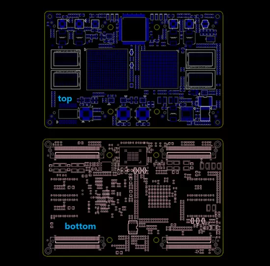
Communication Mainboard PCB — High-Density BGA Fanout Design Lattice CPLD + TI FPGA · 4 Bottom-Plate Connectors · 3× Differential · Mid-Board Cutouts · 10–14 Layers · Superb Automation
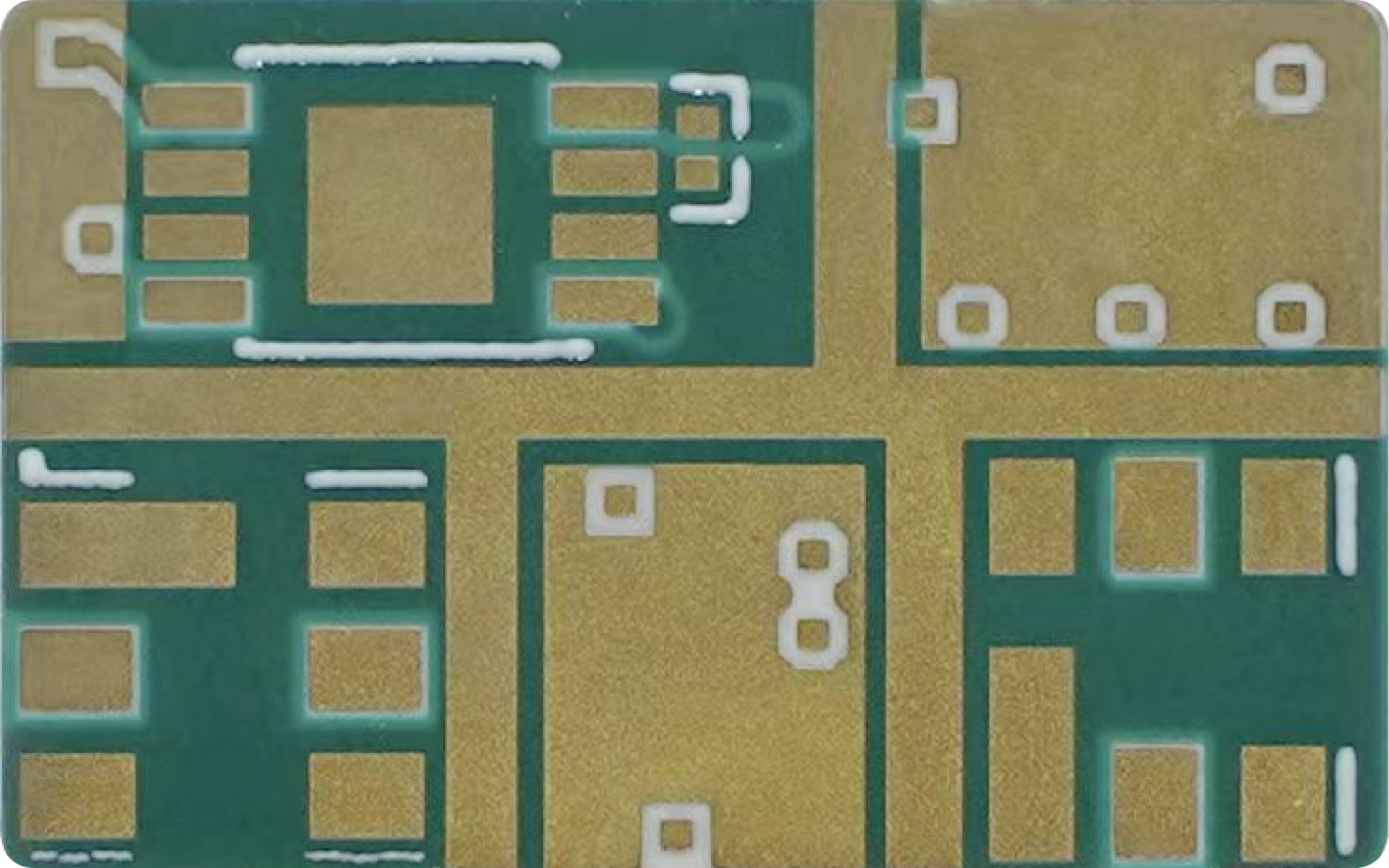
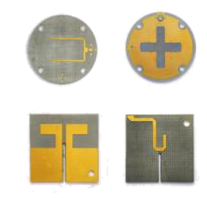
2-Layer High-Frequency Microwave PCB High-frequency microwave PCB on PTFE laminate. 2 layers, 0.127–5.0 mm thickness range, 1 × 3 mm minimum board size. Microwave transmission line width tolerance ± 0.015 mm. Full-board ENIG soft gold plus localized thick gold 2 μm. Planar resistor integration and laser cutting.

 English
English
English