01
DFM Review
Engineering team checks your Gerber files before production starts - report in 24h.

 English
Engineering team checks your Gerber files before production starts - report in 24h.
Dry film lamination -> LDI exposure -> develop -> etch -> strip for circuit formation.
Automated optical inspection verifies inner layer patterns before lamination.
Copper surface preparation for strong inter-layer bonding reliability.
Stack cores + prepregs -> heat & pressure -> multilayer bonding up to 68 layers.
CNC mechanical drill (0.15mm+) + laser micro-via (0.1mm) - aspect ratio up to 20:1.
Cleans hole walls & activates PTFE/polyimide - essential for high-frequency materials.
Chemical copper deposition on hole walls - creates conductive base for electroplating.
Same LDI process applied to outer copper - trace/space down to 2/2 mil.
Electrolytic copper plating + tin etch resist - builds trace thickness to spec.
Remove unwanted copper - leaving only the designed circuit pattern intact.
LPI coating -> exposure -> development -> thermal cure. Standard green, custom colors.
ENIG / Lead-Free HASL / OSP / Immersion Silver / Immersion Tin - matched to your design.
Component reference designators, polarity marks, logos - white, black or yellow ink.
Flying probe or bed-of-nails - 100% net coverage: continuity & isolation verified.
V-scoring or CNC routing to final board shape - clean edges, precise dimensions.
Visual + dimensional check -> vacuum sealed -> labeled & ready to ship.
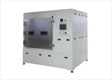
Universe solder mask blasting pretreatment GL231108B1025A (1 unit). Surface preparation before solder mask for optimal coating adhesion and zero bubbles.
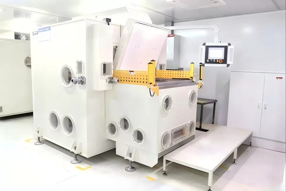
When Chemistry Fails, Physics Takes OverStandard FR-4 desmear uses aggressive permanganate chemistry - it etches epoxy resin smear from hole walls beautifully. But it fails complet
Taiyo & Tamura LPI solder mask. Apply, expose, develop, cure. Green standard; black, white, blue, red available. Precision dam formation between fine-pitch pads.
CEDATE (Italy) & HuoQuan vacuum lamination presses. Precision multilayer bonding up to 68 layers. Temperature and pressure controlled for void-free lamination.
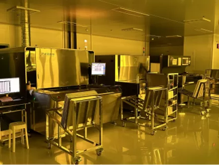
LDI fine-line exposure down to 2/2 mil trace/space. Synova S100807 (2 units) utilizing UV laser direct writing. Eliminates phototool for HDI precision with zero film alignment erro
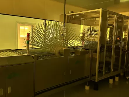
Schmid & KCE dry film laminators for photoresist application on inner and outer layers. Horizontal and vertical coating with uniform thickness control.
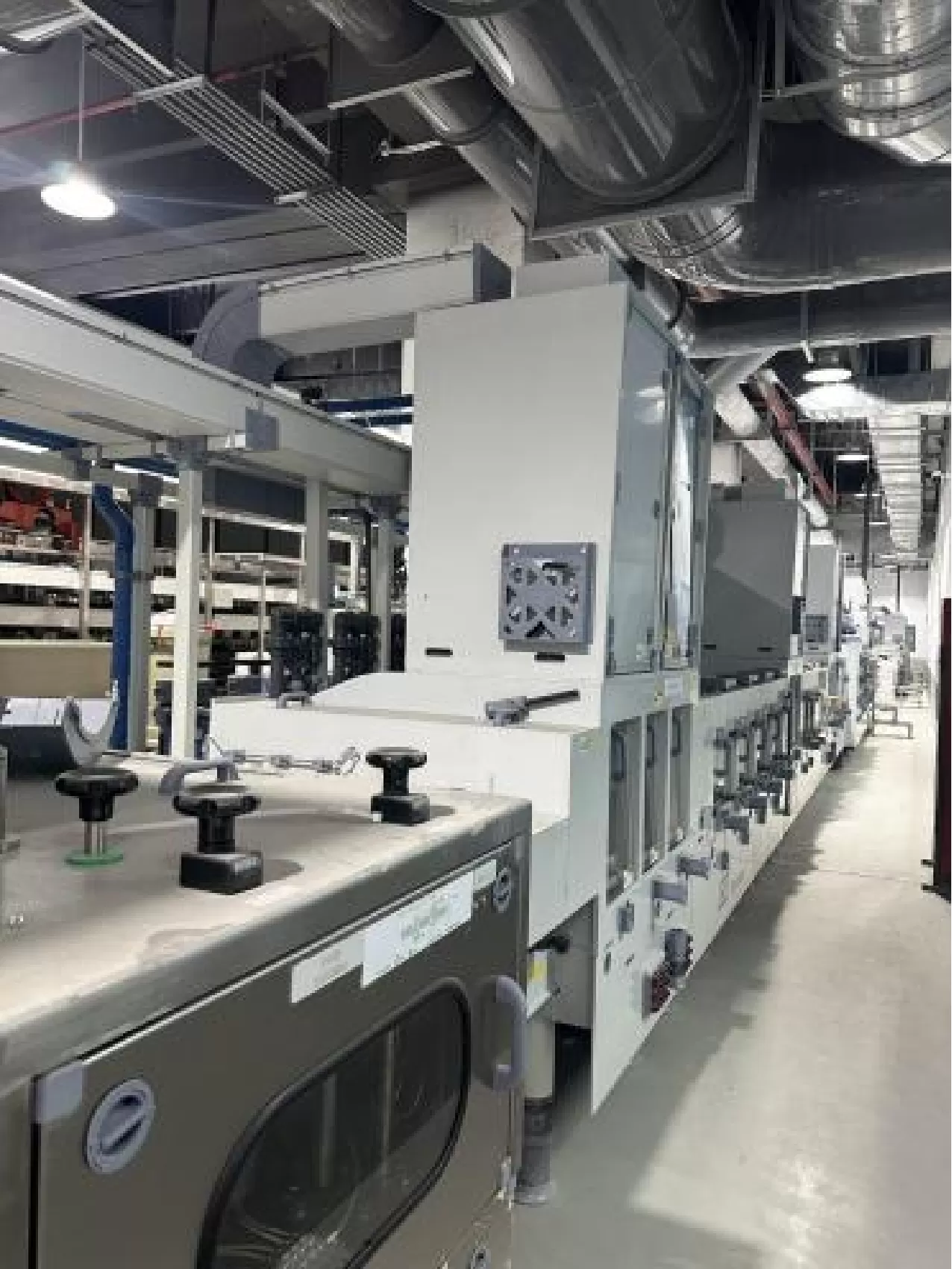
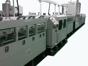
DES acid etching line GL231108B1027A (1 unit). 3 dedicated lines for Develop-Etch-Strip with real-time process monitoring.
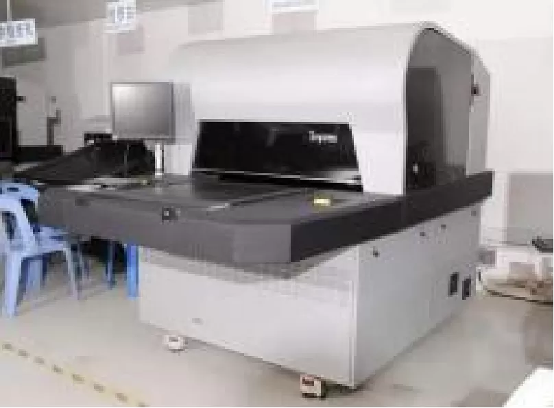
10 AOI stations (Orbotech Discovery/Spiron) catch shorts, opens & pattern defects on inner layers before lamination. Prevents costly multilayer scrap.
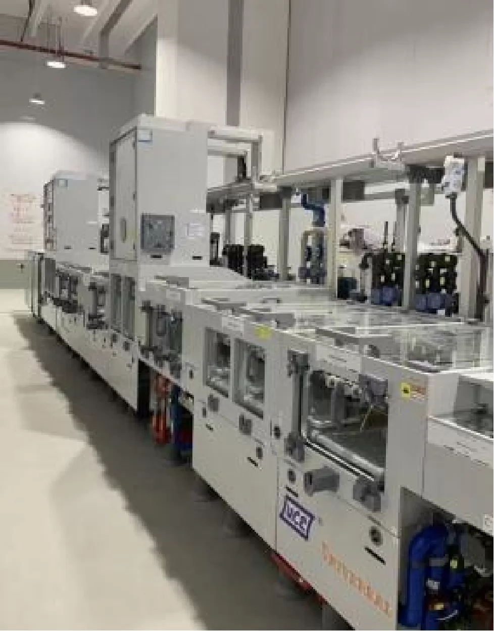
ChuangKe & DengTai oxide treatment lines. Brown/black oxide copper surface preparation for maximum interlayer bonding in multilayer lamination.
In-house silkscreen printers for legend - component IDs, polarity marks, logos. White, black, or yellow ink. Permanent epoxy-based marking.
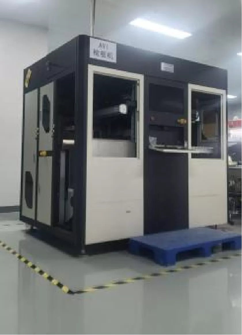
40 inspection stations for visual check, dimensional measurement, vacuum packaging. Every board examined per IPC-A-600 before shipment.
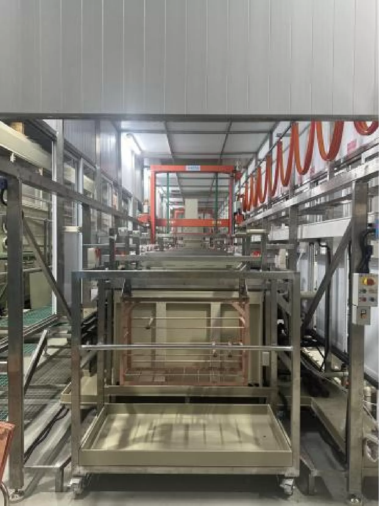
Universe copper deposition pretreatment line GL231108B1032A + Atotech electroless copper. Chemical copper deposition creates conductive base for electrolytic plating.
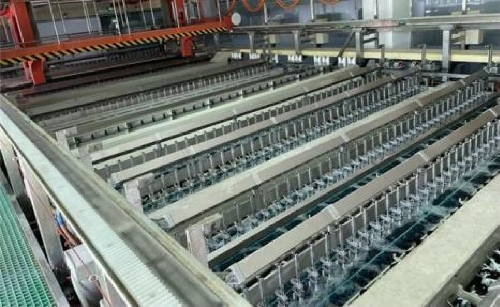
Dongwei vertical continuous plating line (8 copper) + Atotech/Schmid. Electrolytic copper plating to target thickness with heavy copper support for power electronics.
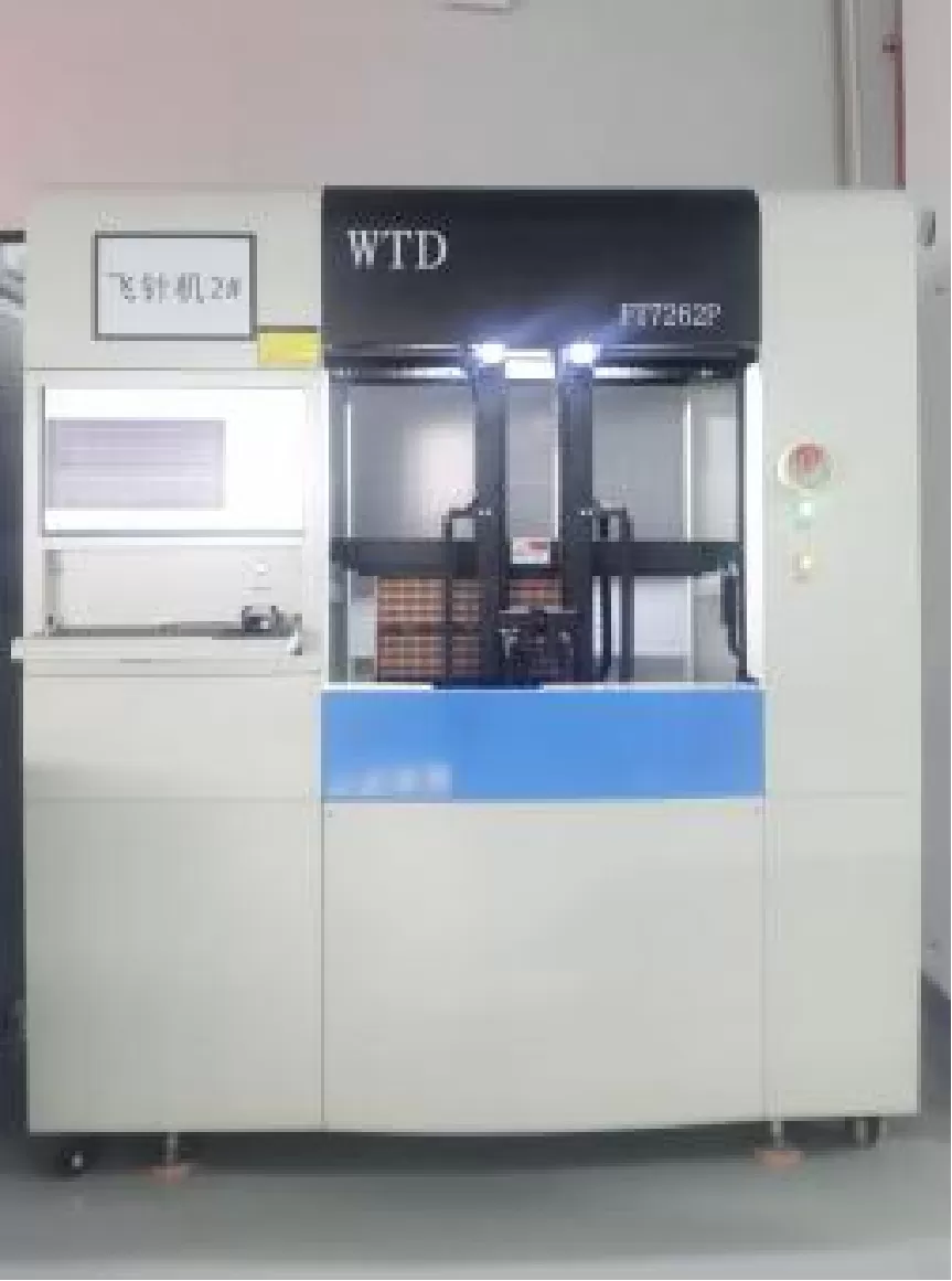
Wangtongda fully automatic tester GL231108B1045A + ATG flying probe. 100% net coverage without custom fixture. Fast prototype turnaround.
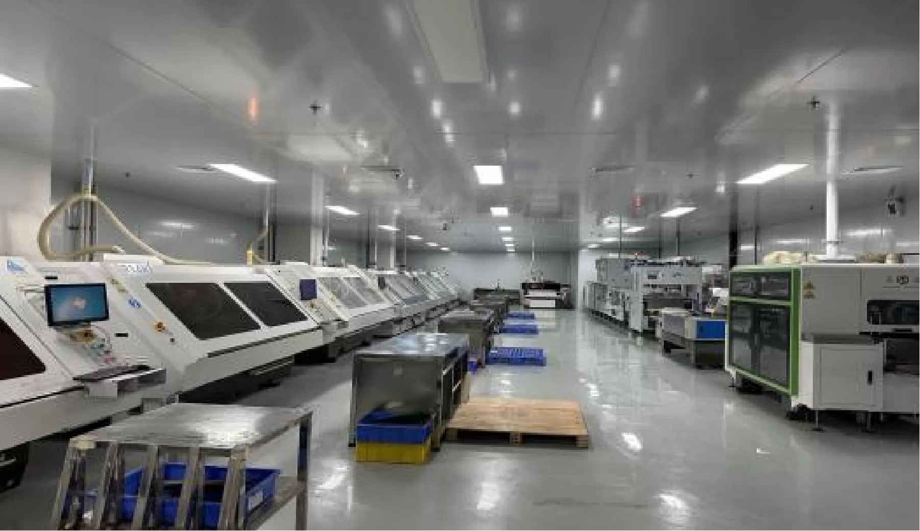
Shenghai single-blade V-CUT machine + YOWSUN. PCB profiling, depaneling & edge beveling. V-scoring for panelized boards, CNC routing for complex shapes.
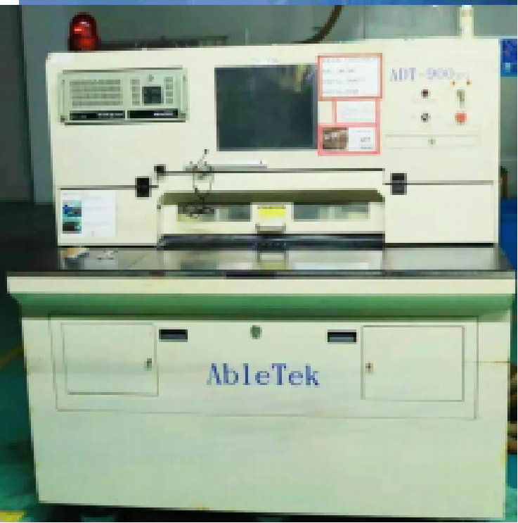
Taiwan Haoshuo X-Ray drilling target machine ADT-900. Precision X-ray drill target positioning for multilayer PCB layer-to-layer registration accuracy.
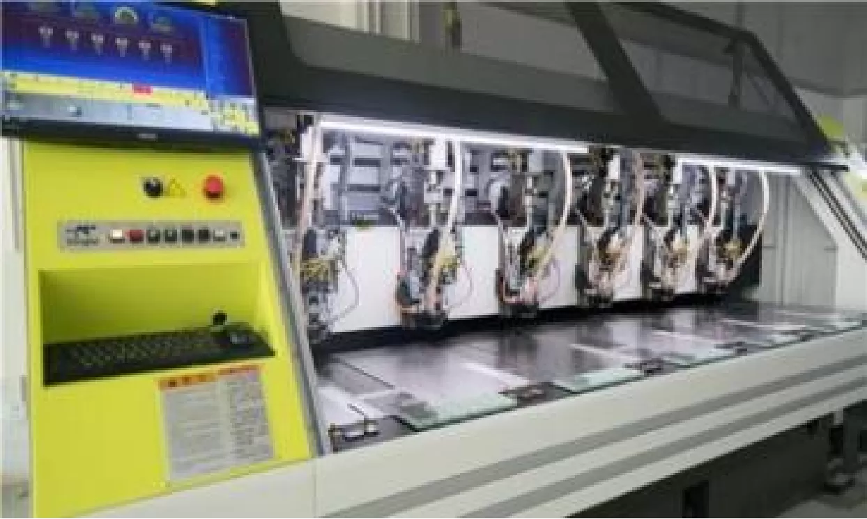
CNC drilling machines including Taiwan Tongtai SD-62C 200,000 RPM (2 units), Hitachi, DongTai. Mechanical drilling down to 0.15mm, aspect ratio 20:1. 150+ spindles across our PCB w
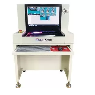
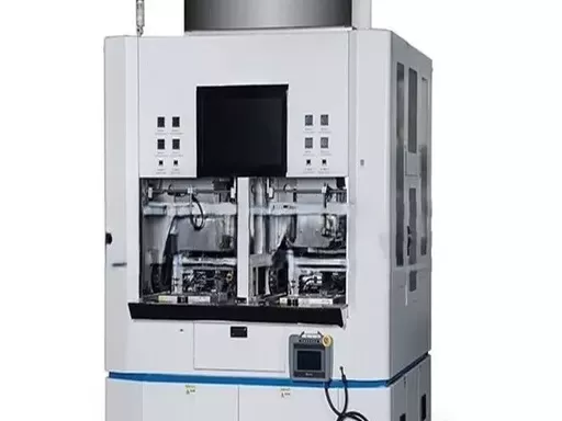
Final AOI scan verifies solder mask coverage, pad alignment & legend quality after all processing. Last automated gate before electrical test.
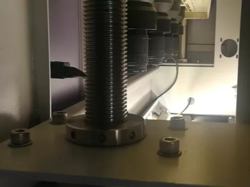
10 AOI stations catch shorts, opens & pattern defects on inner layers before lamination. Prevents costly multilayer scrap.
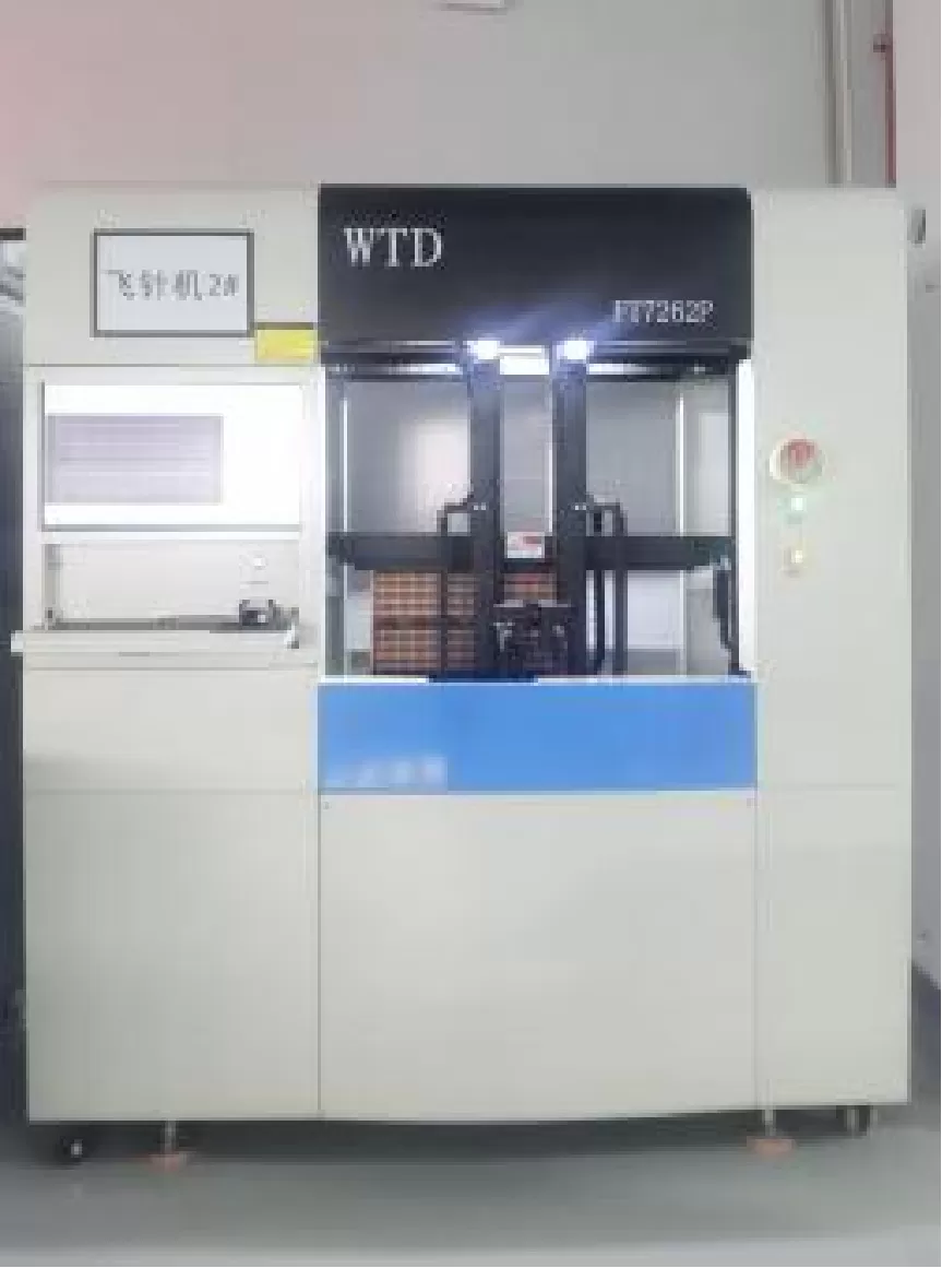
ATG flying probe testers. Continuity and isolation on every net, no fixture needed. 6 machines for fast prototype and production turnaround.
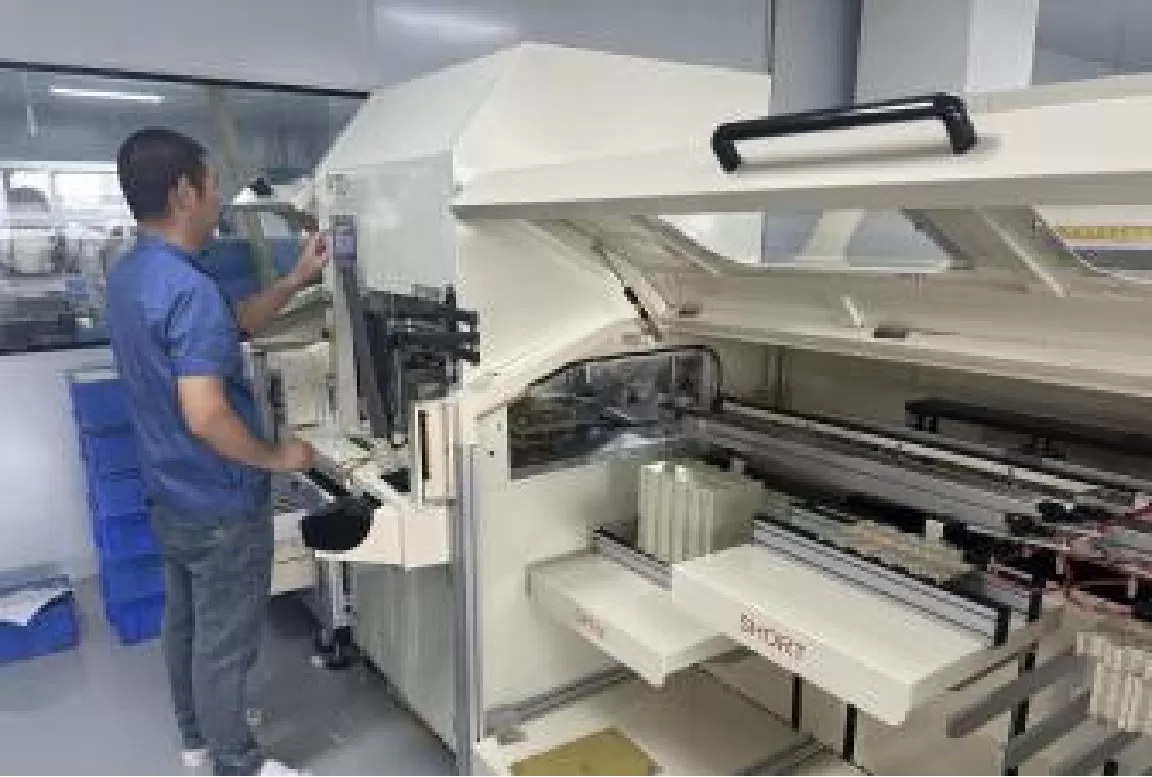
10 dedicated bed-of-nails test stations for high-volume PCB production. Custom fixture contacts every test point simultaneously. Test time under 3 seconds per board.
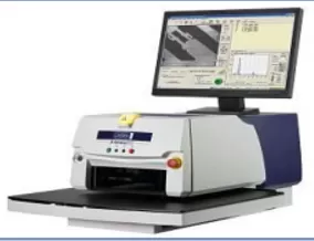
Non-destructive X-ray inspection for internal PCB defects - voids, delamination, drill registration. Sub-micron precision for multilayer verification.
Cross-section analysis with Olympus microscope. Plating thickness, hole wall quality, inter-layer bonding. Destructive testing for process validation per IPC-6012.
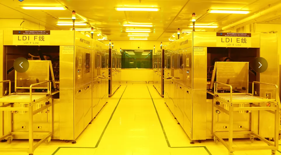
288C solder float test per IPC-TM-650 verifies PCB resistance to assembly thermal shock. Pass/fail: no delamination or hole wall separation.

Solderability test per IPC-J-STD-003 verifies surface finish wetting. Ensures perfect solder acceptance at your assembly line. Tests every finish type.
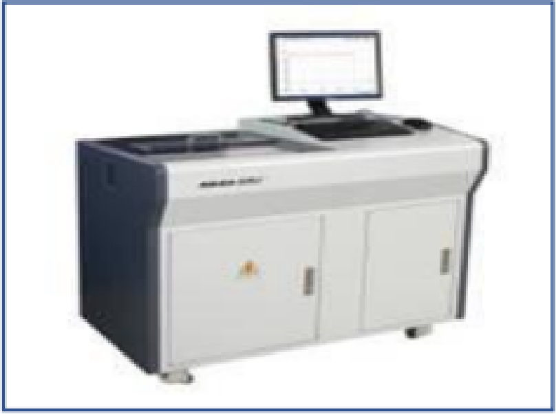
ROSE testing per IPC-TM-650 2.3.25 measures residual ionic contamination. Ensures long-term reliability against corrosion and electrochemical migration.
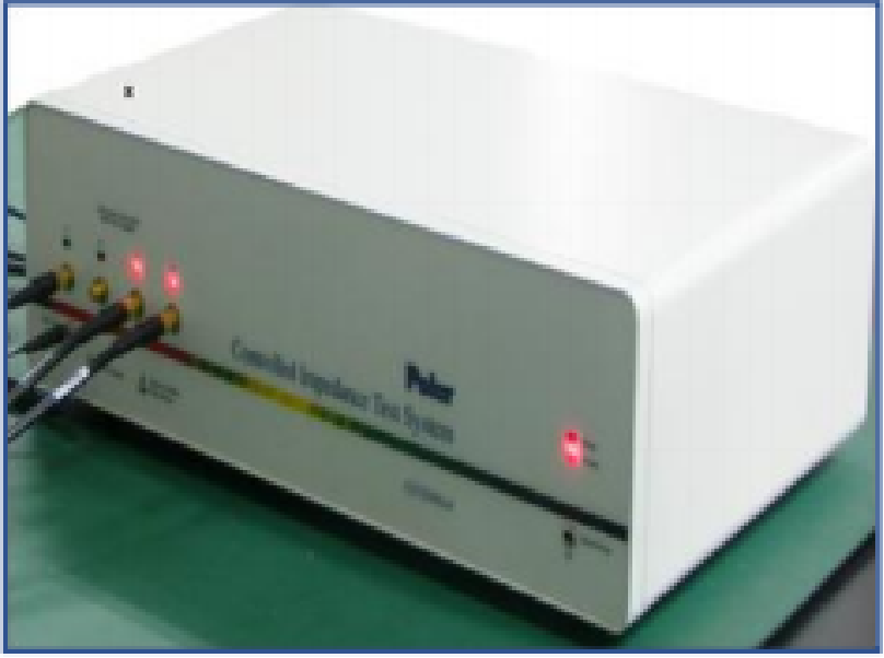
TDR verifies controlled impedance accuracy on every production panel. +/-10% standard, +/-5% available. Critical for RF and high-speed digital.
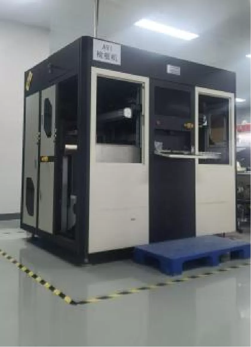
40 inspection stations. Magnified visual check, dimensional verification, vacuum packaging. Every board to IPC-A-600 before shipment.
Step inside our PCB manufacturing facility - 200+ high-precision machines, from drilling to final inspection.
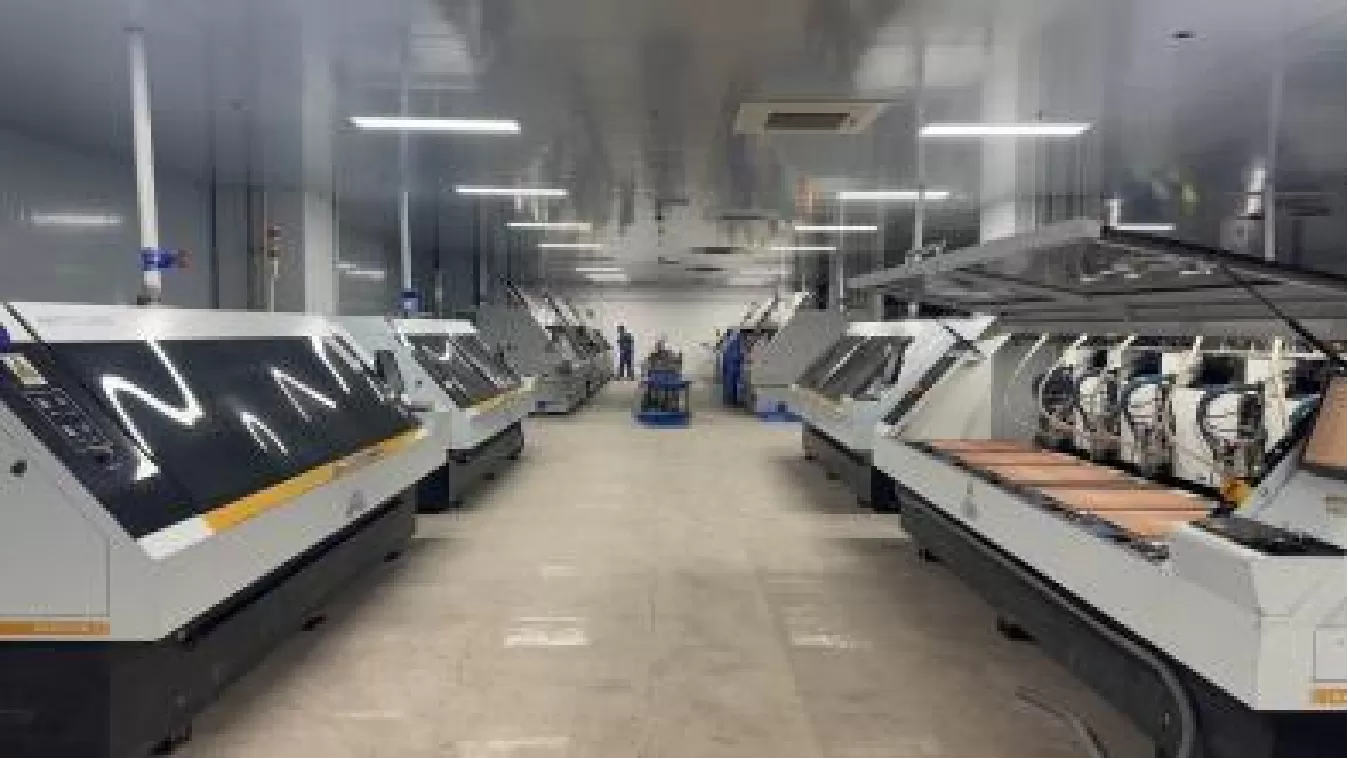
High-speed CNC drilling workshop: 150+ spindles including Taiwan Dongtai SD-62C 200,000 RPM (2 units). Mechanical drilling to 0.15mm, aspect ratio 20:1.
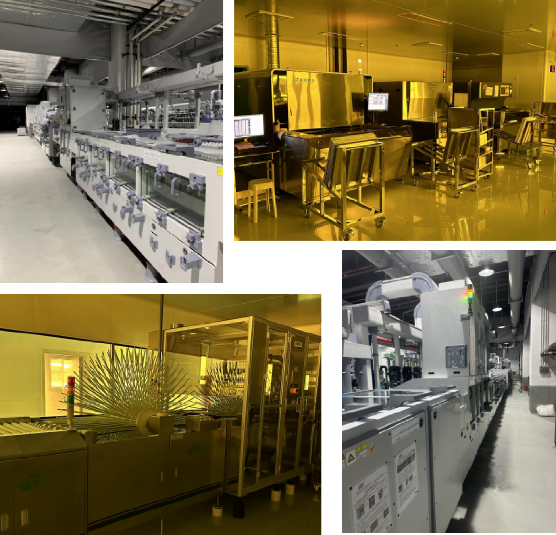
xinuo LDI Automatic exposure machine S100807 (2台) for fine-line exposure. 2/2 mil trace/space. Laser direct writing eliminates film errors.
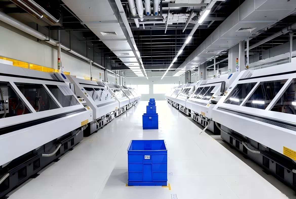
Full PCB factory walkthrough: drilling to packaging. 200+ machines. See where your boards are made.
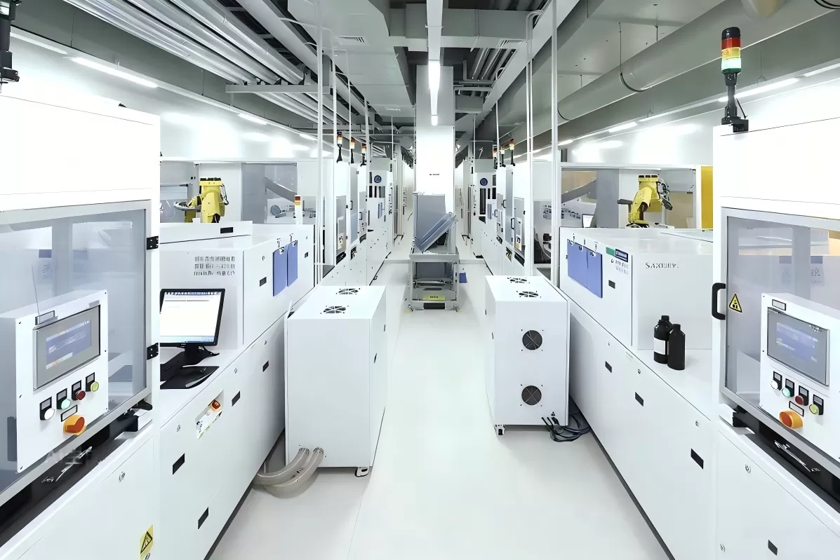
20 Mitsubishi laser drills for micro-via processing. Hole sizes to 0.1mm. Dedicated HDI production bay for smartphones and ADAS boards.
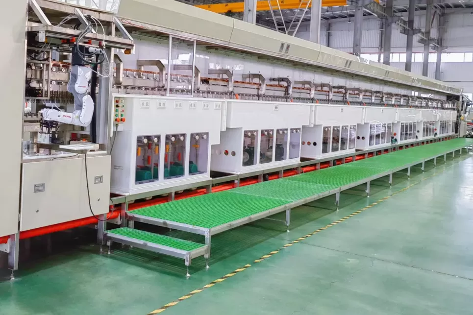
Atotech ENIG line. Electroless Nickel Immersion Gold - flat solderable finish for fine-pitch BGA, wire bonding. XRF verified.
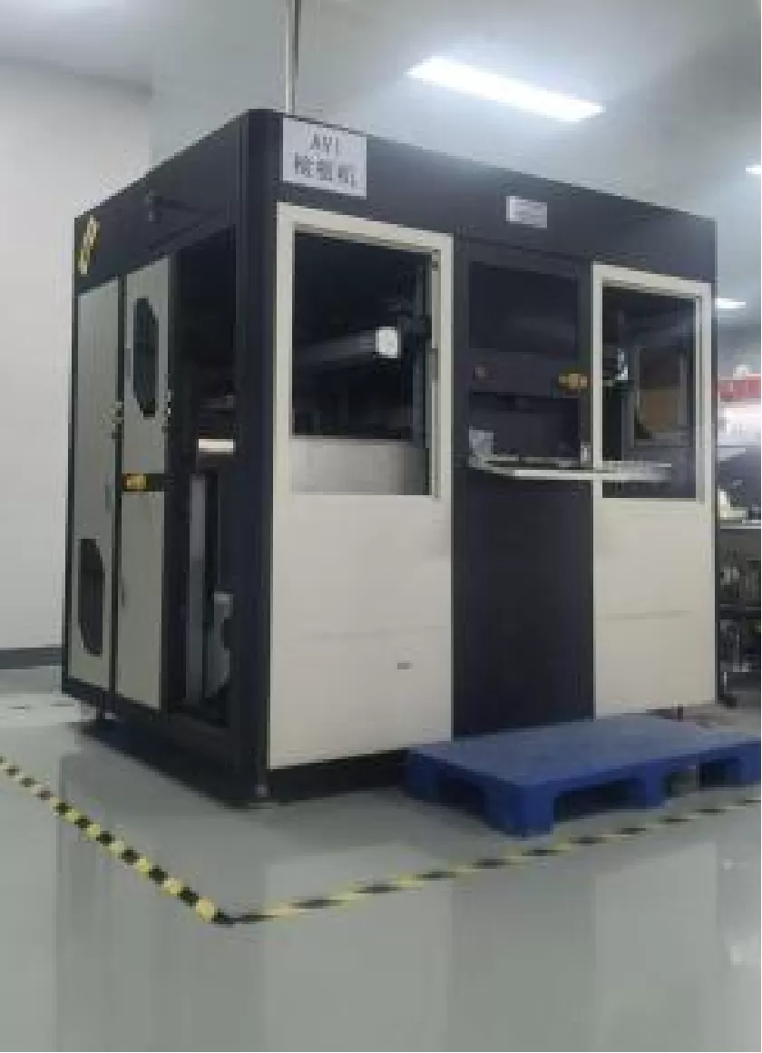
40 inspection stations. Visual check under magnification, dimensional verification, vacuum-sealed packaging. Ready to ship.
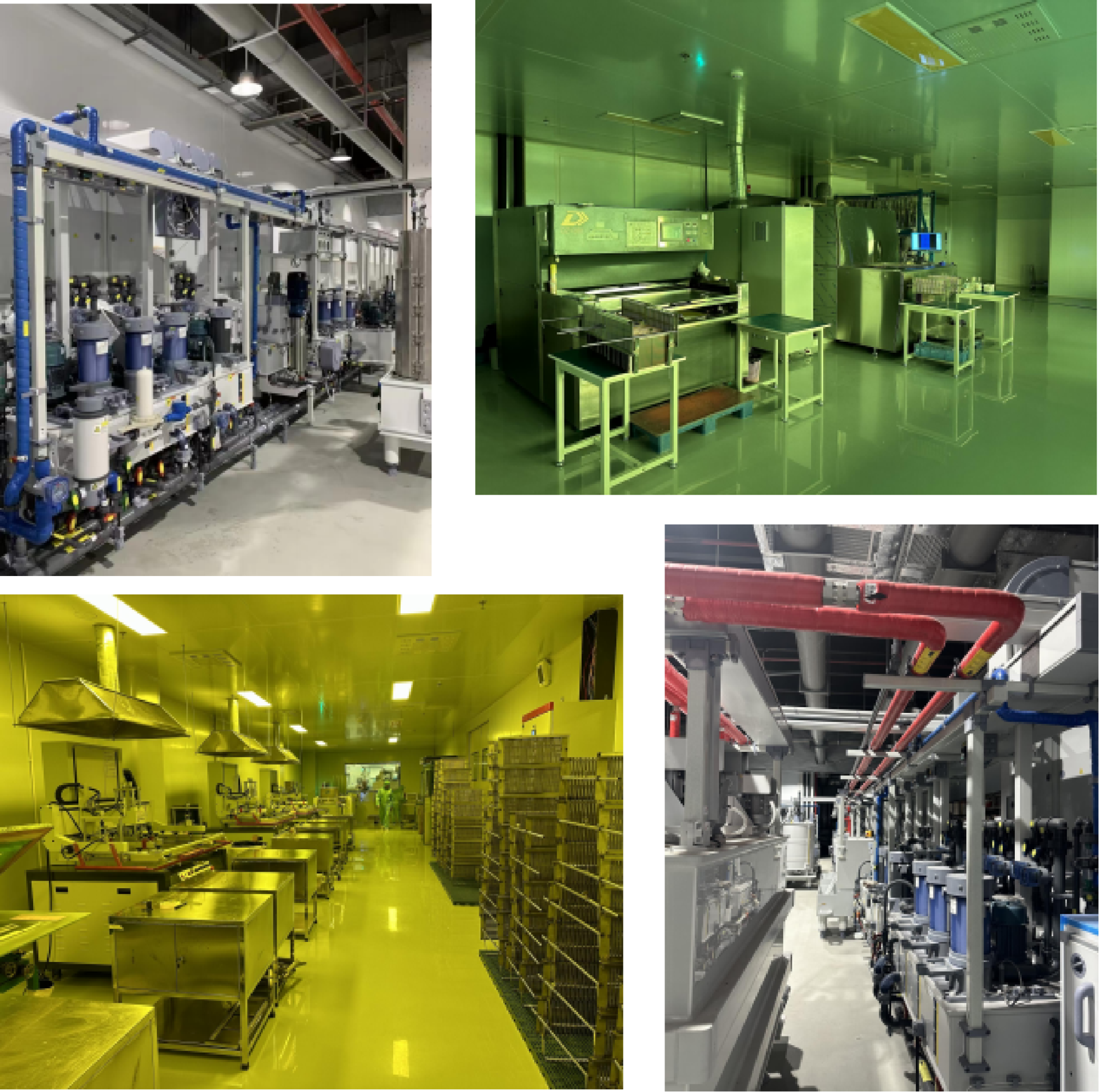
LPI solder mask application, exposure, curing. Silkscreen legend for component identification. Pre-treatment of aerospace assembly for sandblasting ensures perfect adhesion.
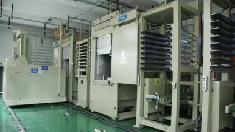
CEDATE vacuum lamination presses + HuoQuan. Stack-up to 68 layers under precise temperature, pressure, and vacuum control.
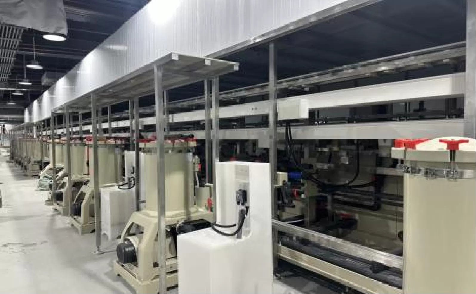
Copper plating pretreatment for galvanized copper plating + Dongwei vertical continuous electroplating line (8 copper).Consistent thickness across all hole walls. Heavy copper supp
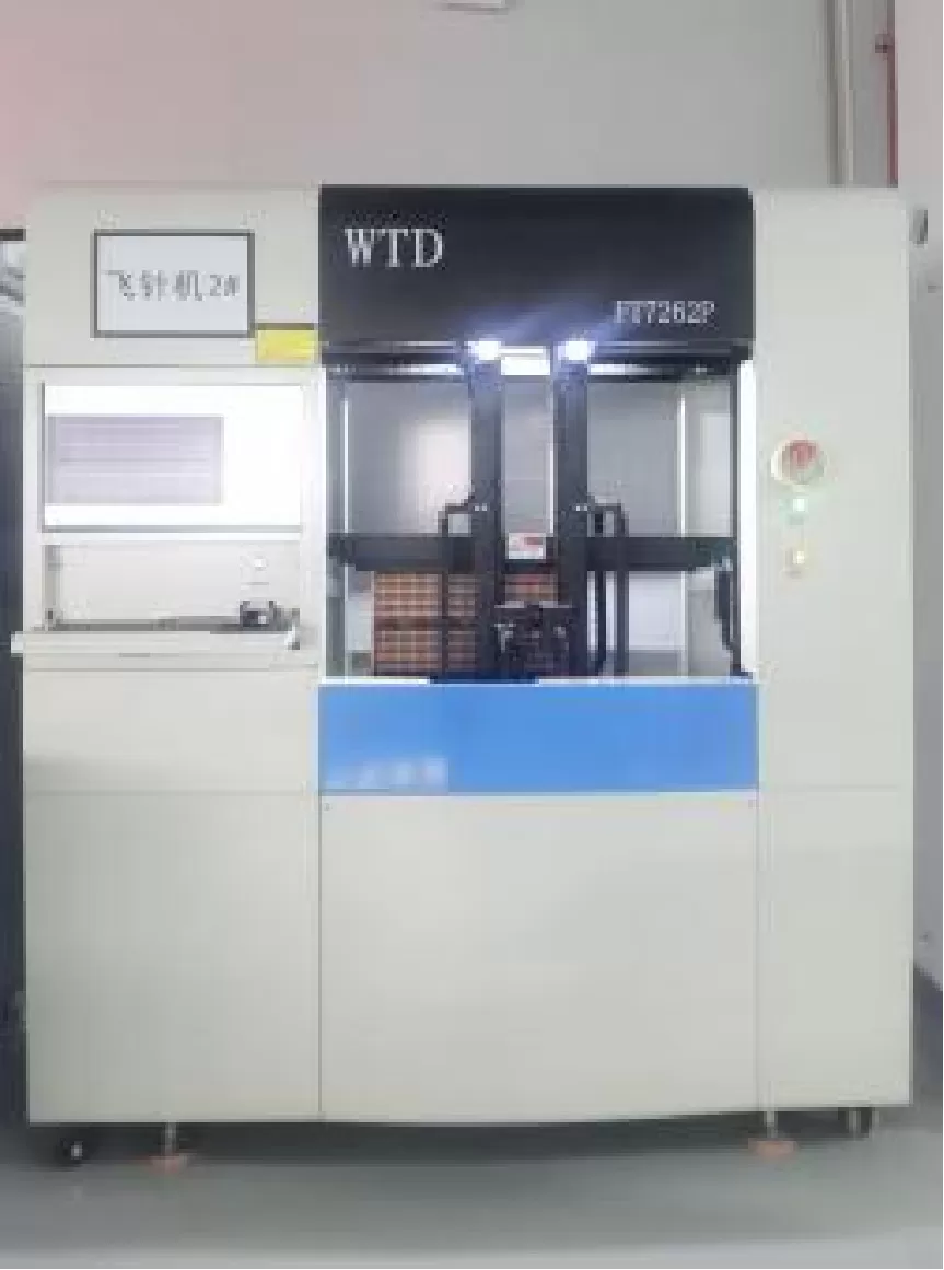
10 AOI stations + WTD flying probe + bed-of-nails fixtures. Every board optically and electrically tested before shipping.
Every PCB is manufactured and inspected to these industry standards - no exceptions.

RoHS-compliant lead-free HASL standard. ENIG per IPC-4552 for fine-pitch. Immersion Ag, Sn, OSP also available.
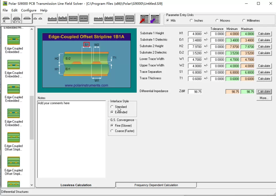
Controlled impedance +/-10% standard, +/-5% for demanding RF and high-speed designs. TDR-verified on every production panel.
IPC-A-600 defines visual acceptance criteria for bare PCBs. Class 2 for industrial/commercial, Class 3 for aerospace, medical & military.
IPC-6012 defines qualification and performance requirements for rigid PCBs: plating, etching, solder mask, tolerances.
Industry-standard test methods per IPC-TM-650: thermal stress, solderability, ionic contamination, microsection, peel strength, impedance.
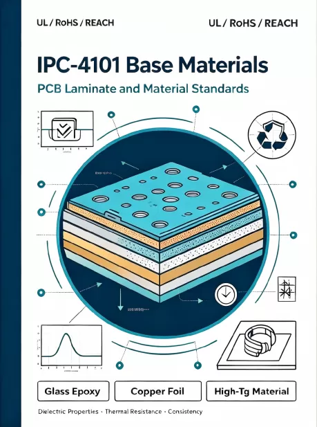
IPC-4101 governs laminate and prepreg properties. Materials from Isola, Rogers, Taconic, Shengyi verified to IPC-4101 slash sheets.
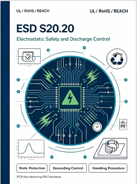
Full ESD protection: grounded workstations, ionizers, conductive flooring, dissipative packaging. Every PCB handled in ESD-safe environment.

All PCB materials UL-recognized, RoHS-compliant (EU 2015/863), REACH-compliant. Material declarations and certificates with every order.