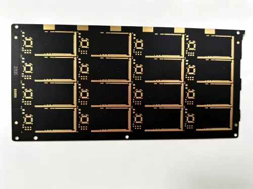
Multilayer High-Speed IC Package Substrate PCB SUPERB provides advanced multilayer high-speed IC package substrate PCB solutions for 5G RF antenna modules, main-frequency power modules and high-frequency processor IC packaging. Featuring multi-layer, multi-step any-layer interconnection technology with Rogers and Panasonic high-performance materials, our substrates enable high-density signal transmission, superior high-frequency performance and reliable semiconductor packaging.
BT Resin IC Package Substrate PCB Solution Advanced Multi-Layer BGA Package Substrate for CPU, Power Module and Processor IC Applications. With the rapid development of semiconductor technology, traditional PCB solutions cannot meet the requirements of high-density chip packaging. IC Package Substrate has become a critical connection platform between semiconductor dies and main PCB systems.
Automotive Telematics PCB Manufacturer — HDI & RF PCB for GPS Tracker, CAN Bus & IoT From 4-layer GNSS tracker boards to 12-layer ADAS camera HDI stacks, Superb Automation fabricates PCBs for telematics, vehicle electronics, and industrial IoT. Our PCB capabilities cover the full range: Rogers RF laminates for GPS/cellular front-ends, high-Tg FR4 for under-hood CAN modules, HDI microvias for miniature asset trackers, and hybrid stacks for multi-radio IoT gateways. 1–68 layers, prototype to 50K/month volume.
16-Layer High Density Multilayer PCB Manufacturing for Precision Electronic Systems Superb manufactures high density multilayer PCB including 16 layer PCB, complex stack-up PCB, signal integrity controlled PCB and precision PCB assembly solutions.
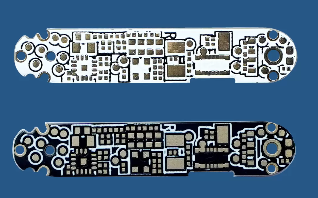
Bluetooth Earphone PCB — 8L 2-Step, ENIG | Superb Automation 8-layer 2-step HDI · 6.52 × 5.21 mm · 0.75 ± 0.08 mm · ENIG · Resin plug · Stacked laser via · White solder mask · 75 μm solder bridge · SMT assembly · Build-to-print from Gerber
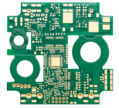
14-Layer 6-Step HDI — High-Voltage Power Transformer Module 14-layer 6-step HDI · 70 μm heavy copper · PTFE+FR4 · 2.5 mm · AC withstand > 2000 V · ENIG · Layer offset < 30 μm · Stacked laser via · Build-to-print from Gerber
Heavy Copper / High-Thermal PCB Fabrication Heavy copper PCB manufacturing — 16 layers · 5 oz inner copper · 3.75 mm · Press-fit ±0.05 mm · Resin plug · Blind via · Build-to-print from Gerber files
Multilayer Backplane PCB — 10G Signal Integrity Simulation 10+ Pairs 10G Signals | System-Level Backplane SI Simulation | Connector Supplier Coordination | Functional Test Passed
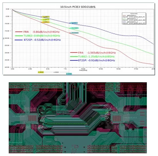
Communication Board Signal Integrity Simulation 60,000 Pins | SFP+ · Interlaken · QPI · PCIe3 · DDR4 · DDR3 | TU872SLK-sp | Intel Platform Loss Spec | 1-Month Turnaround
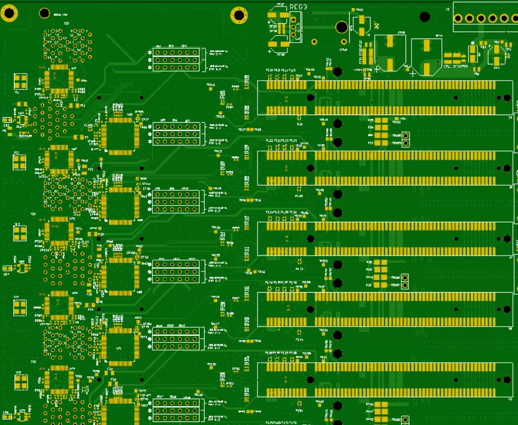
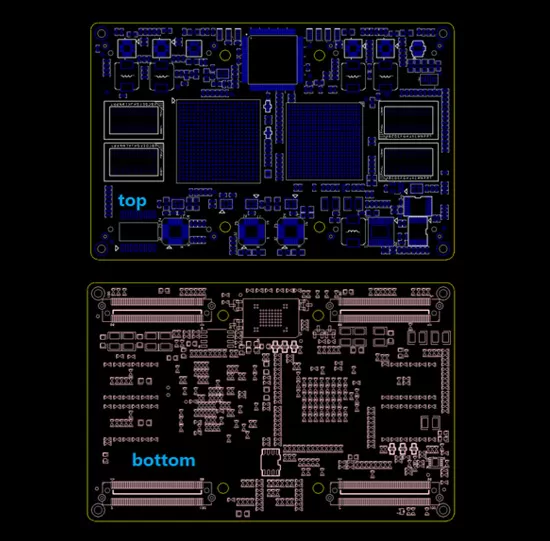
Communication Mainboard PCB — High-Density BGA Fanout Design Lattice CPLD + TI FPGA · 4 Bottom-Plate Connectors · 3× Differential · Mid-Board Cutouts · 10–14 Layers · Superb Automation


 English
English
English