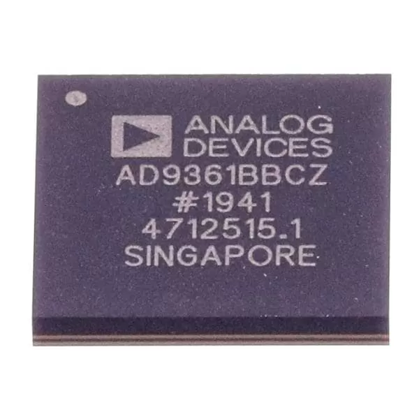
ADG1636BRUZ
Brand: Analog Devices
Analog Devices ADG1636BRUZ is a analog & mixed-signal component designed for Instrumentation and related applications. In stock at Superb Automation — request a quote for competitive pricing and fast delivery.
Product Specifications
ADG1636BRUZ
Analog Devices — Analog & Mixed-Signal ICs
Product Overview
The ADG1636BRUZ from Analog Devices is a high-performance analog / mixed-signal IC providing precision signal acquisition, conversion, and conditioning. Analog Devices (ADI) is a world leader in high-performance analog, mixed-signal, and DSP ICs for instrumentation, healthcare, automotive, and communications.
Superb Automation partners with leading brands including Qorvo, TI, ADI, XILINX, NVIDIA, Intel, ST, MACOM, Renesas, and Coilcraft to provide complete BOM and supply-chain solutions.
Key Features
- High-resolution data conversion with excellent SNR and THD
- Wide dynamic range and high linearity across operating conditions
- Integrated voltage reference with low temperature drift
- Flexible digital interface — SPI, I2C, or parallel options
- Industrial/automotive temperature range with guaranteed specs
- Low power consumption with power-down modes
Key Specifications
| Resolution | bits |
| Channels | — |
| Sample Rate | kSPS |
| Interface | — |
| Supply Voltage | V |
| Operating Temp | °C |
| Package | — |
| INL | LSB |
| SNR | dB |
| THD | dB |
Applications
Precision Instrumentation
Industrial Process Control
Medical Imaging & Diagnostics
Automotive Sensor Interfaces
Communications Infrastructure
Test & Measurement
Request Quote — In Stock, 100% New & Original, Full Warranty
ADG1636BRUZ: 1 Ohm On Resistance, but 238 mA of Channel Current in the TSSOP
The ADG1636 is a dual single pole double throw CMOS switch with one ohm typical on resistance, and it is one of the few parts in this class that publishes the continuous current per channel separately for its two packages. The TSSOP body that the BRUZ code uses is rated 238 mA per channel, while the 4 mm by 4 mm LFCSP reaches 385 mA. A board that carries a 300 mA loop current through the switch works in the LFCSP and fails in the TSSOP, and the difference is in the package table rather than in the front page features.
The on resistance figure and its flatness
One ohm is the typical value at 25 C on a plus and minus 5 V supply. Over the full temperature range the maximum is 1.6 ohm, and the flatness across the analog signal range is 0.2 ohm, which is the number that decides distortion rather than the absolute value. A 0.2 ohm change across the signal swing into a 1 kohm load is 0.02 percent of gain change, and the data sheet pairs that with a total harmonic distortion plus noise figure of 0.007 percent, which is why the part is used for audio routing and for gain switching in data acquisition rather than only for relay replacement.
Supplies, thresholds and the missing logic rail
The switch runs from a 3.3 V to 8 V dual supply or a 3.3 V to 16 V single supply, and the digital inputs are 3 V logic compatible with a 2.0 V minimum input high and a 0.8 V maximum input low. There is no separate logic supply pin to bring up, which removes one rail and one sequencing question from the board. The analog signal range reaches both supplies in the on state, and in the off state signal levels up to the supplies are blocked, so the switch does not need a clamp ahead of it on a signal that swings to the rail.
| Item | Published value | What it decides |
|---|---|---|
| On resistance | 1 ohm typ, 1.6 ohm max over temperature | Insertion loss and gain error |
| Flatness | 0.2 ohm | Distortion across the swing |
| Charge injection | 130 pC typ | Step into a hold capacitor |
| Transition time | 130 ns typ, 209 to 273 ns max | Switching rate ceiling |
| Channel current, TSSOP | 238 mA | Package choice for a current loop |
Charge injection sets the sample and hold error
130 pC of charge injection into a 10 pF hold capacitor is 13 V of step before any correction, and into a 1 nF capacitor it is 130 mV. That is why the same switch is fine as an audio router and needs care in front of an analog to digital converter: the error is set by the capacitor on the far side, not by the switch. The break before make delay is 30 ns typical with a 17 ns minimum, so a multiplexer built from two of these channels has a genuine dead time and the amplifier behind it sees an open input for that window.
Switching speed and crosstalk
Transition time is 130 ns typical, the enable time is 119 ns typical and the disable time is 182 ns typical, so a channel can be cycled at a few hundred kilohertz and no faster. The minus 3 dB bandwidth is 25 MHz and channel to channel crosstalk is 90 dB at 1 MHz, which is the number to check when two channels carry a weak signal next to a strong one. Off leakage is 0.1 nA typical and the on leakage is under a few nanoamps maximum, both small against a 1 kohm load.
Choosing between the two bodies
The LFCSP buys current headroom and board area and costs a thermal pad that has to be soldered, so it is not a drop in against the TSSOP footprint. The pin to pin cross reference page covers which switch families share a pinout, the amplifier cross reference page covers the parts that usually sit behind the switch, and incoming lot checks follow the incoming inspection plan.