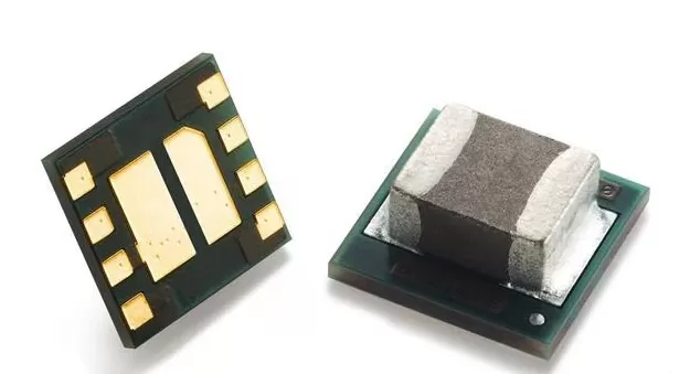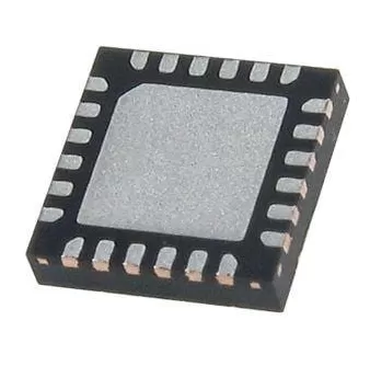

TPS54427DDAR
Brand: Texas Instruments
Texas Instruments TPS54427DDAR is a power management component designed for AI Servers & Low-Altitude Economy (Drone and UAV) and related applications. In stock at Superb Automation — request a quote for competitive pricing and fast delivery.
Product Specifications
TPS54427DDAR
Texas Instruments — Power Management & Signal Chain
Product Overview
The TPS54427DDAR from Texas Instruments is a power management / signal chain IC delivering high efficiency, precision regulation, and robust protection. Texas Instruments (TI) is a global leader in analog ICs, power management solutions, and embedded processors.
Superb Automation partners with leading brands including Qorvo, TI, ADI, XILINX, NVIDIA, Intel, ST, MACOM, Renesas, and Coilcraft to provide complete BOM and supply-chain solutions.
Key Features
- High-efficiency power conversion with low quiescent current
- Wide input voltage range with precision output regulation
- Integrated over-current, over-temperature, and short-circuit protection
- Small footprint packaging for space-constrained designs
- AEC-Q100 qualified options available for automotive applications
- Flexible sequencing and soft-start control
Key Specifications
| Input Voltage | V |
| Output Voltage | V |
| Output Current | A |
| Switching Frequency | kHz |
| Efficiency | % |
| Quiescent Current | µA |
| Topology | — |
| Package | — |
| Operating Temp | °C |
| Protection | — |
Applications
Industrial Automation
Automotive Electronics
Telecom Infrastructure
Server & Data Center Power
Medical Devices
Consumer Electronics
Request Quote — In Stock, 100% New & Original, Full Warranty
TPS54427DDAR: 4.5 V to 18 V input, 4 A synchronous step down converter in an SO PowerPAD body
TPS54427DDAR is a 4 A synchronous step down converter that runs from a 4.5 V to 18 V rail without external compensation in a SO PowerPAD body of 8 pins. The control loop is an adaptive on time scheme with no external compensation network, so the parts count around the device is an inductor, two capacitors and the feedback divider. Output voltage is set between 0.76 V and 7 V, the switching frequency is fixed at 650 kHz, and the reference is trimmed to 765 mV typical.
Order code and package
| TPS54427DDA | 8-pin SO PowerPAD (DDA), 75-piece tube, -40 C to 85 C |
| TPS54427DDAR | 8-pin SO PowerPAD (DDA), 2500-piece large reel |
| TPS54427DRCR | 10-pin VSON (DRC), 3.00 mm by 3.00 mm, 3000-piece large reel |
| Marking, DDA and DRC rows | 54427 |
| Switching frequency | 650 kHz, fixed |
Electrical parameters that decide the application
| Input voltage, recommended range | 4.5 V to 18 V, absolute maximum 20 V |
| Output voltage range | 0.76 V to 7 V, set by the feedback divider |
| Feedback threshold | 757 mV minimum, 765 mV typical, 773 mV maximum |
| High side FET on resistance | 70 mOhm |
| Low side FET on resistance | 53 mOhm |
| Continuous output current | 4 A |
| Supply current, not switching | 950 uA typical, 1400 uA maximum at 25 C |
| Shutdown current | under 10 uA |
| EN high level | 1.6 V minimum, EN low level 0.6 V maximum |
| Operating junction temperature | -40 C to 150 C, ambient rating -40 C to 85 C |
What the two bodies change
| DDA, 8 pins | SO PowerPAD, 4.89 mm by 3.90 mm, the body with the larger pad for heat |
| DRC, 10 pins | VSON, 3.00 mm by 3.00 mm, the smaller footprint on the same silicon |
| Pin count difference | the VSON body exposes SW and VIN on two pins each, the SO body uses one |
| Reel and tube | 75 pieces in a tube, 2500 on the DDA reel, 3000 on the DRC reel |
| Thermal path | both bodies rely on the exposed pad soldered to a copper area, the DRC body needs more vias |
Points to check before this part goes on a BOM
The feedback threshold is 765 mV typical and 757 to 773 mV over the full window, which is plus or minus about 1 per cent at 25 C. A 1.2 V rail therefore depends on the divider tolerance as much as on the part, and a 1 per cent resistor pair is the right choice when the rail feeds a memory or a radio that expects 5 per cent total.
The control loop adopts both polymer and ceramic output capacitors, which is the practical reason this family survives a cost reduction cycle. A board that changes from a 100 uF polymer to two 22 uF ceramics does not need a new compensation network, but the output ripple and the transient response do change, and both should be measured after the swap.
The 650 kHz switching frequency is fixed. That removes one variable from the filter choice and puts the first switching harmonic at a known place, which helps when the product has to pass an emissions test with a compact input filter. It also fixes the inductor value: a smaller inductance raises ripple current and the 4 A rating is reached sooner.
The high side FET is 70 mOhm and the low side 53 mOhm, so at 4 A the conduction loss is about 1.1 W in the high side during the on time and less in the low side, and the body has to move that heat through the exposed pad. The SO PowerPAD body spreads it over a larger pad while the VSON body needs a via field under the pad to reach inner copper.
Supply current while not switching is 950 uA typical and 1400 uA maximum, which is high for a standby rail. A product that has to hold a rail alive for a wake circuit should either disable the converter and use a small linear regulator for the housekeeping load, or accept the milliwatt and budget it in the sleep current.
Shutdown current is under 10 uA, so the enable pin is a real off switch. The enable threshold is 1.6 V high and 0.6 V low, which means a 1.8 V logic line can drive it directly and a divider from the input rail can be used for a simple under voltage lockout without an extra supervisor.
Soft start is adjustable and the part supports a pre-biased output, which matters on a rail that is held up by another supply during sequencing. Without pre-bias support, the low side FET would pull the already charged output down at the start of the sequence and the load would see a dip.
Cycle by cycle over current limit protects the inductor and the FETs, but the limit is not a foldback, so a hard short holds the current at the limit until the thermal path gives up or the upstream fuse opens. A product that must survive an indefinite short needs a fuse or a hot swap device ahead of the converter, not just the converter limit.
The ambient rating of the DDA body is minus 40 to plus 85 C while the junction is rated to 150 C. At 4 A in a 5 V to 1.2 V conversion the dissipation is around 1.5 W, and in a small enclosure the ambient rise alone can reach the point where the junction margin is thin, which is the case where the larger DDA pad earns its space.
The two bodies are not footprint compatible. A board that has to accept either one needs a pad that covers the 8 pin SO outline and the 10 pin VSON outline, and the pin numbering differs, so a board that may switch bodies late in the programme should be built for one body and a drop in substitute confirmed against the pin table rather than assumed.
The loop has no external compensation, but it does have minimum on and minimum off times, and at 18 V in with a low output the on time becomes short enough that the loop starts to skip pulses and the ripple grows at that corner. A board that has to hold a 0.9 V rail from an 18 V bus should be measured at that corner rather than assumed from the 4 A rating, because the number on the front page is quoted at a duty cycle where the loop has room to work.
Where this order code fits
It makes the 1.2 V, 3.3 V or 5 V rail in a set top box, a television main board or a network terminal, where the input is a 12 V adapter, the load is a processor or an analogue section, and the board cannot afford a compensation network or a long qualification cycle. Teams comparing it with a neighbouring part start from our Power Management Cross Reference page, and teams replacing a part that has gone end of life start from the Pin to Pin Cross Reference page.
Questions buyers ask
Does this need a compensation network? No. The adaptive on time loop is internally compensated for the range of output capacitors the vendor specifies, so the external parts are the inductor, the input and output capacitors, the bootstrap capacitor and the feedback divider.
What is the real output current at 5 V in and 1.2 V out? The part is rated 4 A, but the current available at a low duty cycle is limited by the minimum on time and by the thermal path. A 5 V to 1.2 V conversion at 4 A dissipates enough to need the larger DDA pad or a good via field under the VSON body.
Can it run from a 19 V laptop adapter? The recommended input range stops at 18 V and the absolute maximum is 20 V. A 19 V adapter sits outside the recommended range even though it is below the absolute maximum, so a 19 V rail needs a different member of the family with a higher rating.
SUPERB holds and sources this line for production and repair demand, quoted against the exact ordering string with date codes, packing and country of origin stated on the offer. When a part is moving, the How to Reduce Component Cost page sets out the checks that keep a substitute from failing on the bench.