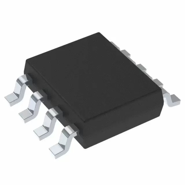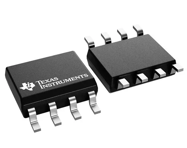

INA592IDGKR
Brand: Texas Instruments
Texas Instruments INA592IDGKR is a power management component designed for Industrial Automation and related applications. In stock at Superb Automation — request a quote for competitive pricing and fast delivery.
Product Specifications
INA592IDGKR
Texas Instruments — Power Management & Signal Chain
Product Overview
The INA592IDGKR from Texas Instruments is a power management / signal chain IC delivering high efficiency, precision regulation, and robust protection. Texas Instruments (TI) is a global leader in analog ICs, power management solutions, and embedded processors.
Superb Automation partners with leading brands including Qorvo, TI, ADI, XILINX, NVIDIA, Intel, ST, MACOM, Renesas, and Coilcraft to provide complete BOM and supply-chain solutions.
Key Features
- High-efficiency power conversion with low quiescent current
- Wide input voltage range with precision output regulation
- Integrated over-current, over-temperature, and short-circuit protection
- Small footprint packaging for space-constrained designs
- AEC-Q100 qualified options available for automotive applications
- Flexible sequencing and soft-start control
Key Specifications
| Input Voltage | V |
| Output Voltage | V |
| Output Current | A |
| Switching Frequency | kHz |
| Efficiency | % |
| Quiescent Current | µA |
| Topology | — |
| Package | — |
| Operating Temp | °C |
| Protection | — |
Applications
Industrial Automation
Automotive Electronics
Telecom Infrastructure
Server & Data Center Power
Medical Devices
Consumer Electronics
Request Quote — In Stock, 100% New & Original, Full Warranty
INA592IDGKR: wide bandwidth difference amplifier with gains of one half and two
INA592IDGKR is a difference amplifier with selectable gains of one half or two in a VSSOP body of 10 pins. A difference amplifier is not an instrumentation amplifier: it takes a differential signal and refers it to a single ended output with a fixed gain, and it does so with 40 microvolts of offset and 88 dB of rejection. The 10 pin VSSOP body carries the gain select pins, and the part runs from 4.5 V to 36 V single or plus and minus 2.25 to 18 V.
Order code and package
| Order code | INA592IDGKR |
| Function | difference amplifier, gains of one half and two |
| Package | VSSOP, 10 pins |
| Other bodies | 8 pin MSOP and 8 pin SOIC |
| Supply | 4.5 V to 36 V single, plus and minus 2.25 to 18 V |
| Gain error | 0.03 percent maximum |
| Offset voltage | 40 microvolts maximum |
| Common mode rejection | 88 dB minimum |
| Bandwidth | 2 MHz gain bandwidth product |
| Slew rate | 18 volts per microsecond |
| Load drive | 500 picofarads |
| Datasheet | SBOS914 revision F |
Electrical parameters that decide the application
| Offset drift | 2 microvolts per C maximum |
| Noise | 18 nanovolts per root hertz at 1 kHz |
| Quiescent current | 1.1 milliamps per amplifier |
| Input impedance | set by the internal network, not by a pair of external resistors |
| Common mode range | extends to the supply rails with the internal divider |
| Temperature range | minus 40 to plus 125 C |
| Gain options | one half for attenuation, two for gain |
| Output | single ended, referred to the reference pin |
| Settling | 18 volts per microsecond slew with a 500 picofarad load |
| Comparison | tighter offset than a four resistor difference amplifier built from an op amp |
Points to check before this part goes on a BOM
A difference amplifier is not an instrumentation amplifier and the input impedance is the reason. The internal network loads the source, so a high impedance bridge needs a buffer or a different part, while a low impedance shunt is exactly what this stage wants.
Forty microvolts of offset and 2 microvolts per C of drift are the numbers a shunt front end needs. On a 10 milliohm shunt they are 4 milliamps and 0.2 milliamps per C of reading error, which is tighter than most current sense amplifiers in this catalogue.
The gain of one half is not a mistake in the table. Attenuating a plus and minus 10 volt signal into a 3.3 V converter is a legitimate use of a difference amplifier, and it is why the part offers both ratios.
The internal resistors are matched on the die, which is what buys 88 dB of rejection. Four external 0.1 percent resistors around an op amp reach roughly 60 dB, and their ratio drift adds a term the amplifier was bought to remove.
The supply range up to 36 V lets the part sit on a 24 V rail without a regulator, and the dual supply option keeps a plus and minus 15 V signal path in range. The 4.5 V minimum is the limit on the low side, so a 3.3 V rail is not on the list.
Two megahertz of gain bandwidth with 18 volts per microsecond is a general purpose stage and not a fast one. A converter sampling at a megahertz behind this amplifier will see the settling tail long before it sees the bandwidth limit.
Where this order code fits
Current shunt front ends, bridge conditioning and line receivers are the boards that use it, especially where the signal has to be referred to a different ground. Boards comparing it with a neighbouring part start from our Amplifier Cross Reference page, and boards replacing a part that has gone end of life start from the How to Verify a Drop in Replacement page.
Questions buyers ask
How is this different from an instrumentation amplifier? Input impedance and gain range. This part loads the source through its internal divider and offers fixed ratios, while an instrumentation amplifier buffers the inputs and offers a resistor set gain from 1 up.
Can the gain be changed without changing the part? Yes on this version. The 10 pin body carries gain select pins for the one half and two ratios, and the 8 pin bodies are fixed at one ratio each.
SUPERB holds and sources this Texas Instruments line for production and repair demand, quoted against the exact ordering string with date codes, packing and country of origin stated on the offer. When a line is moving, the Supplier Quality Audit page sets out the checks that keep a substitute from failing on the bench.