


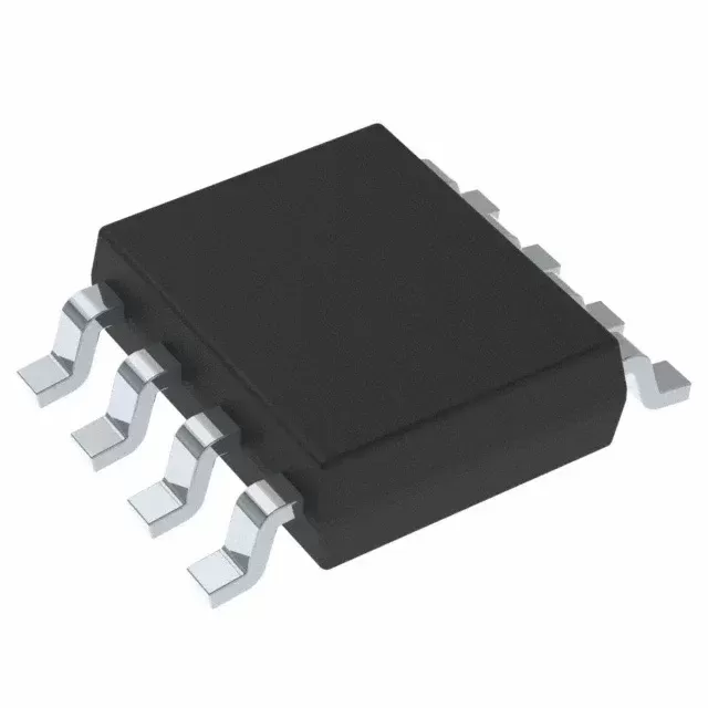
LM5164DDAR
The LM5164DDAR is a wide-input-voltage, 1A synchronous buck DC-DC converter from Texas Instruments — designed to step down voltages from as high as 100V to a regulated output as low as 1.2V, all from a single 8-pin SO PowerPAD package. With integrated high-side and low-side N-channel MOSFETs, constant on-time (COT) control for fast transient response, and an industry-leading sub-10µA no-load quiescent current, it is the go-to regulator for always-on industrial sensors, 48V telecom power supplies, Power-over-Ethernet (PoE) powered devices, and automotive battery-connected electronics where every microamp of standby current counts.
Product Specifications
LM5164DDAR — 100V, 1A Synchronous Buck DC-DC Converter by Texas Instruments
The LM5164DDAR is a wide-input-voltage, 1A synchronous buck DC-DC converter from Texas Instruments — designed to step down voltages from as high as 100V to a regulated output as low as 1.2V, all from a single 8-pin SO PowerPAD package. With integrated high-side and low-side N-channel MOSFETs, constant on-time (COT) control for fast transient response, and an industry-leading sub-10µA no-load quiescent current, it is the go-to regulator for always-on industrial sensors, 48V telecom power supplies, Power-over-Ethernet (PoE) powered devices, and automotive battery-connected electronics where every microamp of standby current counts.
Quick Specifications
| Parameter | Value |
|---|---|
| Manufacturer | Texas Instruments |
| Part Number | LM5164DDAR |
| Mouser # | 595-LM5164DDAR |
| Topology | Synchronous Buck (Step-Down) DC-DC Converter |
| Input Voltage Range (VIN) | 6 V to 100 V |
| Output Voltage (VOUT) | Adjustable: 1.2 V to ~90 V (VIN − Dropout, <1 V at 1A) |
| Output Current (IOUT, Continuous) | 1 A |
| Integrated MOSFETs | High-Side + Low-Side N-Channel (Synchronous Rectification) |
| RDS(ON) — High-Side FET | ~0.45 Ω (Typical, VIN = 24V) |
| RDS(ON) — Low-Side FET | ~0.25 Ω (Typical, VIN = 24V) |
| Control Method | Constant On-Time (COT) with Peak Current Mode |
| Switching Frequency (fSW) | Adjustable: up to 1 MHz (Set via RT Resistor) |
| Quiescent Current (IQ, No-Load) | < 10 µA (Typical, VOUT Regulated, No Switching) |
| Shutdown Current (ISD) | < 2 µA (Typical, EN = Low) |
| Feedback Voltage (VFB) | 1.2 V (±1% Accuracy Over Temperature) |
| Soft-Start | Internal, Fixed ~3 ms Ramp (Typical) |
| Power-Good (PG) Flag | Open-Drain Output, Active High When VOUT > 92% of Target |
| External Clock Sync | Yes — SYNC/MODE Pin for Synchronization to External Clock |
| Over-Current Protection (OCP) | Cycle-by-Cycle Peak Current Limit (~1.5A Valley); Hiccup Mode After 256 Cycles |
| Thermal Shutdown (TSD) | ~175°C (Rising), ~160°C (Falling Hysteresis) |
| Package | 8-Pin SO PowerPAD (HSOIC-8, 3.9 × 4.9 mm, Exposed Thermal Pad) |
| Operating Junction Temperature | −40°C to +125°C |
| Packaging | Tape & Reel (DDAR Suffix, 2,500 pcs/Reel) |
| Automotive Variant | LM5164-Q1 (AEC-Q100 Qualified, Same Electrical Specs) |
| EVM / Development Kit | LM5164DDAEVM (for DDA Package) — Available from TI |
| RoHS | Compliant (RoHS3) |
Product Overview
The LM5164DDAR is a member of TI's wide-VIN synchronous buck converter family — purpose-built for systems where the input voltage is high, unregulated, or subject to significant transients (48V telecom rails, 24V industrial buses, 12V automotive batteries with load-dump spikes up to 60V+). Unlike linear regulators which dissipate (VIN − VOUT) × IOUT as heat, the LM5164's synchronous buck topology achieves 85–92% typical efficiency across most operating conditions — converting a 48V input to 5V at 1A while dissipating less than 0.8W total (IC + inductor losses combined).
The defining feature of the LM5164 is its ultra-low quiescent current — drawing less than 10 µA from the input when the output is in regulation with no load. This enables always-on power supplies for battery-powered IoT sensors, where the regulator must maintain output voltage indefinitely while the MCU sleeps, waking only to take a measurement. A standard buck converter drawing 1–3 mA of quiescent current would drain a small battery in days; the LM5164 extends that to years.
Constant on-time (COT) control provides near-instantaneous response to load steps without the compensation-network complexity of voltage-mode or current-mode PWM controllers. The on-time is set by an external resistor (R_ON), and the valley current is controlled by an internal senseFET — the combination delivers stable operation across the full input voltage range with ceramic output capacitors (no ESR requirement for loop stability).
Key Features & Benefits
6V–100V Input Range — Survives the Worst Automotive and Industrial Transients
The 100V maximum input rating makes the LM5164 suitable for direct connection to:
48V telecom / PoE: Nominal 48V rails (36–57V range) with margin for transients
24V industrial: Factory-floor 24VDC buses with motor-regeneration spikes to 50V+
12V automotive: Cold-crank dips to 6V, load-dump surges to 40V+, and reverse-battery (with external diode)
72V e-bike / e-mobility: Direct battery connection without pre-regulator
Offline auxiliary supplies: Rectified 85–265VAC through a resistor + zener pre-regulator provides a ~80V DC rail for the LM5164
No external surge suppressor or TVS clamp is required for most industrial and automotive transients within the 100V absolute maximum — the LM5164 absorbs them directly.
Sub-10µA No-Load IQ — Years of Battery Life in Always-On Applications
At less than 10 µA of quiescent current with the output in regulation and no load, the LM5164 consumes ~0.5 mW at 48V input — negligible against any practical battery or energy-harvesting source. In a typical IoT sensor node (LM5164 regulating 48V → 3.3V, MCU sleeping 99% of the time, waking once per minute), the regulator's standby power contribution is less than 0.1% of the system energy budget.
Integrated Synchronous Rectification — No External Schottky Diode
Both the high-side (control) and low-side (synchronous) MOSFETs are integrated on the LM5164 die. The low-side FET replaces the external Schottky catch diode required by asynchronous buck converters — eliminating a BOM line item, reducing PCB area, and recovering the diode's forward-voltage-drop power loss (~0.3V × IOUT). At 1A output, synchronous rectification saves approximately 200–300 mW compared to a diode-based design.
Constant On-Time (COT) Control — Fast Transient Response, No Compensation Network
COT control modulates the switching frequency in response to load and line changes while keeping the on-time constant. This enables:
Near-instantaneous load-step response: Output voltage deviation is primarily determined by output capacitance and ESR — not control-loop bandwidth
No external compensation components: No Type-II or Type-III compensation RC networks to calculate, tune, or de-rate over temperature — a significant BOM and design-time savings
Stable with ceramic output capacitors: COT control does not require output-capacitor ESR for loop stability — use low-ESR MLCCs for minimum output ripple
SO-8 PowerPAD Package — Thermally Enhanced for 1A Continuous
The PowerPAD (exposed thermal pad) on the underside of the SO-8 package conducts heat directly into the PCB copper plane — essential for dissipating the ~0.5–1W of power loss at full 1A load. TI recommends a minimum of 2 cm² of 1 oz copper connected to the thermal pad with thermal vias to an internal ground plane for continuous 1A operation at TA = 85°C ambient. Without the PowerPAD connection (i.e., standard SO-8 without thermal pad), the junction temperature would exceed 125°C at 1A load under the same conditions.
Typical Application Circuits — Quick-Start Designs
48V to 5V, 1A — Industrial Sensor Power Supply
| Component | Recommended Value | Part Number Example |
|---|---|---|
| Input Capacitor (CIN) | 2.2 µF + 0.1 µF, 100V, X7R, 1206 | TDK C3216X7R2A225K |
| Output Inductor (L) | 47 µH, 1.5A ISAT, 0.15 Ω DCR | Coilcraft MSS1260-473ML |
| Output Capacitor (COUT) | 22 µF, 16V, X7R, 1210 × 2 | Murata GRM32ER71C226K |
| Feedback Resistors (RFBT/RFBB) | 100 kΩ / 31.6 kΩ (VOUT ≈ 5.0V) | Any 1%, 0402 or 0603 |
| RON Resistor | 100 kΩ (fSW ≈ 300 kHz at VIN=48V, VOUT=5V) | Any 1%, 0402 |
| Bootstrap Capacitor (CBOOT) | 0.1 µF, 16V, X7R, 0603 | Any X7R |
| VCC Capacitor | 1 µF, 16V, X7R, 0603 | Any X7R |
Efficiency at 48V→5V, 1A: ~88% typical. Total power loss: ~0.7W. Junction temperature rise: ~30°C above ambient with 4 cm² copper pour.
24V to 3.3V, 0.5A — IoT Gateway Always-On Rail
| Component | Recommended Value | Part Number Example |
|---|---|---|
| Input Capacitor | 2.2 µF + 0.1 µF, 50V, X7R, 1206 | TDK C3216X7R1H225K |
| Output Inductor | 33 µH, 1A ISAT, 0.2 Ω DCR | Coilcraft LPS6235-333ML |
| Output Capacitor | 22 µF, 10V, X7R, 0805 × 2 | Murata GRM21BR71A226M |
| Feedback Resistors | 100 kΩ / 57.6 kΩ (VOUT ≈ 3.3V) | Any 1%, 0402 |
| RON Resistor | 100 kΩ (fSW ≈ 250 kHz at VIN=24V, VOUT=3.3V) | Any 1%, 0402 |
Efficiency at 24V→3.3V, 0.5A: ~90% typical. Ideal for always-on sensor nodes — 10 µA standby consumption is negligible on a 24V industrial bus.
PCB Layout Guidance — PowerPAD SO-8
The LM5164's SO-8 PowerPAD package requires specific PCB layout attention to achieve rated thermal performance and minimize EMI:
Exposed Thermal Pad: Solder the PowerPAD directly to a copper plane on the top layer. Connect to internal ground plane(s) with 4–6 thermal vias (0.3 mm drill, plated). Minimum 2 cm² of 1 oz copper for 1A at 85°C ambient.
Input Capacitor Placement: Place CIN (2.2 µF + 0.1 µF) within 5 mm of the VIN and GND pins. The high-frequency 0.1 µF capacitor must be closest to the pins. The input current loop (VIN → CIN → PGND) is the most critical high-di/dt path — minimize loop area.
Switch Node (SW): Keep the SW node copper area minimal — just enough to connect the IC pin to the inductor. The SW node swings from 0V to VIN at the switching frequency and is the primary source of radiated EMI. Do not pour copper under the SW node on internal layers.
Feedback Trace: Route VFB as a quiet, narrow trace away from the SW node and inductor. Connect the feedback divider's ground directly to the AGND pin (pin 2), not to the power ground plane — this prevents ground-bounce noise from coupling into the feedback loop.
Bootstrap Capacitor: Place CBOOT (0.1 µF) as close as possible to the BOOT and SW pins — within 3 mm. This capacitor provides the gate-drive voltage for the high-side MOSFET.
LM5164 vs Competing Wide-VIN Synchronous Buck Converters
| Feature | LM5164DDAR (TI) | LMR16006Y (TI) | MP2451 (MPS) | LT8608 (Analog Devices) |
|---|---|---|---|---|
| Input Voltage (Max) | 100 V | 60 V | 36 V | 42 V |
| Output Current | 1 A | 0.6 A | 0.6 A | 1.5 A |
| No-Load IQ | < 10 µA | 28 µA | 120 µA | 2.5 µA |
| Integrated FETs | HS + LS (Sync) | HS + LS (Sync) | HS Only (Async, Needs Diode) | HS + LS (Sync) |
| Sync Input | Yes (SYNC/MODE) | No | No | Yes (SYNC) |
| Power-Good Flag | Yes | Yes | No | Yes |
| Package | SO-8 PowerPAD | SO-8 PowerPAD | TSOT-23-6 | MSOP-10 |
| Control Method | COT (Simple) | COT (Simple) | Voltage Mode (Needs Compensation) | Burst Mode® (Proprietary) |
| Best For | 48V/24V Industrial, PoE | 12V/24V General | Low-Cost 12V | Ultra-Low IQ, Higher IOUT |
Selection guide: The LM5164 wins on input voltage range (100V) and IQ/cost ratio. The LMR16006 is a lower-current, 60V sibling — choose it for <0.5A loads. The MP2451 is a low-cost alternative but requires an external Schottky diode and external compensation. Analog Devices' LT8608 offers the lowest IQ (2.5 µA) and higher current (1.5A) but at significantly higher cost and with a 42V input limit — insufficient for 48V rails.
Target Applications
48V Telecom & PoE Powered Devices (PDs)
The LM5164 is the ideal post-PD-interface buck for IEEE 802.3af/at PoE powered devices. The PoE input (37–57V after bridge rectifier) feeds directly into the LM5164's VIN pin — stepping down to 5V, 3.3V, or 1.8V for the PD's MCU and peripherals. No intermediate LDO or pre-regulator needed.
Industrial 24V Sensor Nodes & IO-Link Devices
IO-Link sensors, 4–20mA loop-powered transmitters, and factory-floor sensor nodes operating from 24VDC rails. The sub-10µA IQ ensures the regulator contributes negligible power draw to the system's standby budget — critical for loop-powered devices where the entire system must operate within the 4mA loop current.
Automotive Always-On Power Supplies
Direct connection to 12V vehicle battery (with reverse-battery protection diode). The LM5164 powers always-on ECUs — keyless entry receivers, telematics control units, and battery management wake-up circuits — where the regulator must maintain output voltage for months without draining the battery.
E-Bike / LEV Motor Controller Auxiliary Supply
E-bike and light electric vehicle (LEV) motor controllers running from 36V, 48V, or 72V battery packs need a low-voltage auxiliary rail (5V or 12V) for the MCU, gate drivers, and communication modules. The LM5164's 100V input handles the full pack voltage with margin for regenerative-braking voltage spikes.
Solar-Powered / Energy-Harvesting Systems
Solar panel outputs (typically 12–48V open-circuit) connect directly to the LM5164, which provides a regulated 3.3V or 5V rail for the charge-controller MCU, even under very light load when the panel is barely illuminated — the 10µA IQ ensures the regulator isn't the dominant load on the panel.
Isolated / Fly-Buck Auxiliary Supplies
In a Fly-Buck configuration, the LM5164 generates an isolated output using a coupled inductor — primary side provides the regulated non-isolated output; secondary side provides an isolated auxiliary rail for gate drivers, isolated RS-485/CAN transceivers, or IGBT/SiC driver bias supplies.
Frequently Asked Questions
What is the difference between LM5164DDAR and LM5164DDAT?
Identical silicon. DDAR = 2,500-unit Tape & Reel (standard production packaging). DDAT = 250-unit small reel (typically for prototype/sample orders). For production, order DDAR. For engineering samples, DDAT is convenient but DDAR is perfectly fine for prototype quantities as well.
What is the difference between LM5164 and LM5164-Q1?
The LM5164-Q1 is the AEC-Q100 qualified automotive variant — same electrical specifications but with additional qualification testing (temperature cycling, ESD, AEC-Q100 Grade 1, −40°C to +125°C TJ). For non-automotive applications, the standard LM5164 is functionally identical and more cost-effective. If your design may later need automotive certification, design with the -Q1 footprint (identical package) and swap the BOM line item when needed.
How do I set the output voltage?
The output voltage is set by two external resistors (RFBT and RFBB) forming a voltage divider from VOUT to the FB pin (1.2V reference). Formula: VOUT = 1.2V × (1 + RFBT / RFBB). Example: RFBT = 100kΩ, RFBB = 31.6kΩ → VOUT = 1.2 × (1 + 100/31.6) ≈ 5.0V. Use 1% tolerance resistors. The minimum output voltage is 1.2V (FB connected directly to VOUT, RFBB = open).
How do I set the switching frequency?
Connect a resistor (RON) from the RON pin to VIN. The on-time is proportional to RON and inversely proportional to VIN: tON ≈ RON × (VOUT / VIN). For a target switching frequency at a given operating point, use TI's LM5164 Quick-Start Calculator (Excel) or Webench Power Designer to calculate the RON value. Typical values: RON = 100kΩ gives fSW ≈ 200–400 kHz depending on VIN/VOUT ratio.
Does the LM5164 require an external Schottky diode?
No. The LM5164 is a synchronous buck converter — the low-side integrated MOSFET replaces the external catch diode. An external Schottky is not required during normal operation. However, TI recommends a small Schottky diode (e.g., 1A, 100V) from SW to GND only if the LM5164 is used in a Fly-Buck (isolated) configuration, where the diode handles the secondary-side rectification.
What is the minimum order quantity (MOQ)?
Contact SUPERB Automation for a tailored quote. The LM5164DDAR ships in 2,500-unit tape-and-reel — we support partial reel quantities for prototyping and small production runs. Send your BOM to pcba@superb-tech.com — we quote within hours.
Ordering Information
| Orderable Part Number | Package | Packaging | Qty / Reel |
|---|---|---|---|
| LM5164DDAR | SO-8 PowerPAD (HSOIC-8) | Tape & Reel | 2,500 |
| LM5164DDAT | SO-8 PowerPAD (HSOIC-8) | Tape & Reel (Small Reel) | 250 |
| LM5164QDDARQ1 | SO-8 PowerPAD (HSOIC-8) | Tape & Reel | 2,500 |
| LM5164DDAEVM | Evaluation Board | — | 1 (EVM) |
Design Resources
Datasheet: LM5164 Datasheet (SNVSBD6) — 29 pages: full electrical characteristics, typical performance curves, application design examples, and PCB layout guidelines
TI Webench Power Designer: Online design tool — enter VIN, VOUT, IOUT, and Webench generates a complete schematic with BOM, efficiency curves, and PCB layout recommendations. Free; no login required
LM5164 Quick-Start Calculator: Excel-based calculator for RON resistor selection, inductor value, output capacitor, and compensation-free stability check
Evaluation Module: LM5164DDAEVM — Fully assembled and tested evaluation board with 48V→5V default configuration. Order through TI.com or SUPERB Automation
IBIS Model: Not applicable (analog power IC; use SPICE model below)
SPICE / TINA-TI Model: Unencrypted PSpice transient model available on TI.com — simulate startup, load step, line transient, and efficiency under your exact operating conditions
Application Notes:
SNVA829 — "Designing With the LM5164 Wide-VIN Synchronous Buck Converter"
SNVA999 — "LM5164 PCB Layout Guidelines for Low EMI"
SNVA830 — "Fly-Buck Converter Using the LM5164" (isolated auxiliary supply design)
Request a Quote
SUPERB Automation supplies genuine Texas Instruments LM5164DDAR synchronous buck converters. From partial-reel prototype quantities to full 2,500-unit reels for production, we deliver — along with complementary power components (inductors, capacitors, Schottky diodes, and the LM5164DDAEVM evaluation module) for a complete power-supply BOM.
Send your BOM or inquiry to pcba@superb-tech.com — we quote within hours. Include your target VIN/VOUT/IOUT and we'll also recommend the optimal inductor and capacitor part numbers for your application.
SUPERB Automation — We Make It Real. Since 2000.