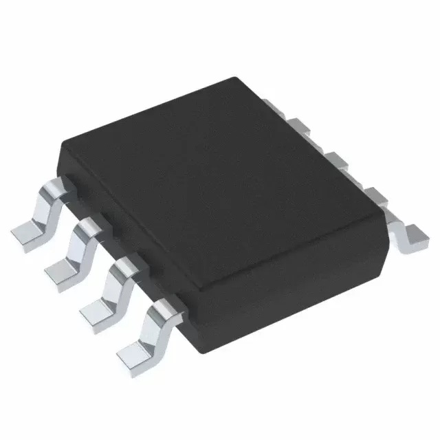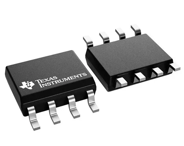

INA322EA-250
Brand: Texas Instruments
Texas Instruments INA322EA-250 is a power management component designed for Industrial Automation and related applications. In stock at Superb Automation — request a quote for competitive pricing and fast delivery.
Product Specifications
INA322EA-250
Texas Instruments — Power Management & Signal Chain
Product Overview
The INA322EA-250 from Texas Instruments is a power management / signal chain IC delivering high efficiency, precision regulation, and robust protection. Texas Instruments (TI) is a global leader in analog ICs, power management solutions, and embedded processors.
Superb Automation partners with leading brands including Qorvo, TI, ADI, XILINX, NVIDIA, Intel, ST, MACOM, Renesas, and Coilcraft to provide complete BOM and supply-chain solutions.
Key Features
- High-efficiency power conversion with low quiescent current
- Wide input voltage range with precision output regulation
- Integrated over-current, over-temperature, and short-circuit protection
- Small footprint packaging for space-constrained designs
- AEC-Q100 qualified options available for automotive applications
- Flexible sequencing and soft-start control
Key Specifications
| Input Voltage | V |
| Output Voltage | V |
| Output Current | A |
| Switching Frequency | kHz |
| Efficiency | % |
| Quiescent Current | µA |
| Topology | — |
| Package | — |
| Operating Temp | °C |
| Protection | — |
Applications
Industrial Automation
Automotive Electronics
Telecom Infrastructure
Server & Data Center Power
Medical Devices
Consumer Electronics
Request Quote — In Stock, 100% New & Original, Full Warranty
INA322EA-250: the low cost five times front end on a 250 piece reel
INA322EA-250 is the low cost member of the family in the 8 pin MSOP on a 250 piece small reel: a gain of 5 built into the package, extendable with one external resistor pair, 40 microamps per channel, under 1 microamp in shutdown, and a supply range of 2.7 to 5.5 volts.
It is not a precision part and the page says so plainly. The offset is 2 millivolts typical and 10 millivolts maximum, the rejection is 73 dB typical, and the gain error at 5 is 0.07 per cent. What it delivers for that is a differential front end with a trimmed gain, a wide temperature range of minus 55 to plus 125 degrees, and a price that makes it the default choice for a sensor whose span is measured in volts rather than millivolts.
INA322EA-250 as the vendor document publishes it
| Quiescent current | 40 microamps per channel |
| Shutdown current | under 1 microamp |
| Internal gain | 5 V/V, with external resistors added through the gain pins |
| Gain equation | 5 plus 5 multiplied by the ratio of the two external resistors |
| Gain range | 5 to 1000 |
| Gain error at 5 | 0.07 per cent typical, 0.4 per cent maximum |
| Gain drift | 2 ppm per degree typical, 10 maximum |
| Nonlinearity | 0.004 per cent of full scale |
| Offset voltage | 2 millivolts typical, 10 millivolts maximum |
| Offset drift | 7 microvolts per degree |
| Input bias current | 0.5 picoamps typical, 10 picoamps maximum |
| Common mode rejection | 60 dB minimum, 73 dB typical |
| Bandwidth at 3 dB | 500 kHz at a gain of 5 |
| Slew rate | 0.8 volts per microsecond |
| Output swing to the positive rail | 20 millivolts |
| Supply range | 2.7 volts to 5.5 volts |
| Common mode range at 5 volts | 0.55 volts to 3.8 volts |
| Common mode range at 2.7 volts | 0.35 volts to 1.5 volts |
| Body | MSOP, 8 pin, DGK, 3.00 by 3.00 millimetres |
| Temperature range | minus 55 to plus 125 degrees |
| Vendor status | active, 250 piece small reel |
| Catalogue code | INA322EA-250 |
| Vendor string | INA322EA/250, printed with a slash |
| Internal gain | 5 V/V, trimmed |
| Marking | C22 |
| Moisture level | level 2, 260 degrees, one year floor life |
Five volts per volt is built in, the rest is one resistor pair
INA322EA-250 is configured internally for a gain of 5, and any gain above that is set by two external resistors as 5 plus 5 times their ratio. The internal five is trimmed, which is why the part can be used at a gain of 5 with no external network at all, and the external pair extends the range to about 1000.
The arrangement is convenient for a channel that has two gain settings: the fixed 5 for a high level sensor and an external pair for a low level one, with the same part on both. It also means the gain error at 5 is 0.07 per cent while the gain at any external setting is dominated by the resistors, and the drift of the external pair adds to the 2 ppm per degree of the internal network. A 100 ohm potentiometer at the gain pins is therefore a production trim and a temperature drift term at the same time.
Two millivolts of offset, and what that rules out
The offset of INA322EA-250 is 2 millivolts typical and 10 millivolts maximum, with a drift of 7 microvolts per degree. That is a millivolt class part, not a microvolt class part, and it sets the smallest signal the channel can measure without a calibration step: a 20 millivolt full scale bridge has 10 per cent of offset on the typical part and 50 per cent on the maximum one.
The row is not a defect, it is the price of the low cost position. A channel that measures a thermistor with a 2 volt span, a position sensor with a 5 volt span or a line receiver with a 1 volt differential signal never sees the offset, and for those channels the part is the cheapest way to get a differential front end with a trimmed gain of 5. Reading the offset before the sensor span is chosen is the whole of the selection: if the span is above about 200 millivolts, the offset is under 5 per cent of it.
What the low cost position gives up against the INA321
INA322EA-250 and the INA321 share a package, a pinout, a supply range and a quiescent current of 40 microamps, and they differ in the four rows that decide a purchase: offset 2 millivolts typical against 200 microvolts, rejection 73 dB typical against 94, gain error 0.07 per cent at 5 against 0.02, and the internal gain of 5 that the 322 has and the 321 does not.
Those differences are why the two parts are not interchangeable on a board even though the footprint is. A channel that was qualified with the 321 and re-sourced to the 322 loses a factor of ten in offset and 21 dB in rejection, and the symptom appears as a reading that is fine on the bench and wrong in the enclosure. A substitution in the other direction costs money and changes the gain equation from 5 plus 5 times the ratio to 5 times the ratio, so the resistor values have to be recomputed. Our BOM scrubbing page covers that check against the bill of materials.
Sixty decibels of rejection, and the frequency where it holds
The common mode rejection of INA322EA-250 is 60 dB minimum and 73 dB typical, and the family description puts the useful rejection up to about 3 kHz. A 60 dB figure attenuates a 1 volt common mode to 1 millivolt at the input, which at a gain of 5 is 5 millivolts at the output, so a channel that sits on a noisy ground has to keep the common mode below a volt or accept that error.
Where the rejection holds is a different question from its value. The 3 kHz figure comes from the same architecture that gives the part its 500 kHz bandwidth: the rejection is set by resistor matching in the input divider, and the matching degrades as the parasitic capacitance across those resistors takes over at higher frequency. A 50 Hz or 60 Hz line harmonic is well inside the band, a switching supply at 500 kHz is not, and a channel that has to reject a 500 kHz common mode needs an input filter rather than a better amplifier.
Where a fixed gain of five fits
INA322EA-250 fits a thermistor or position sensor front end, a differential line receiver with gain, an automotive sensor interface that has to survive minus 55 to plus 125 degrees, and a low cost bridge channel whose full scale is above 200 millivolts. In each of those the offset is a small part of the signal and the trimmed gain of 5 removes a resistor pair from the board.
It stops where the signal is small or the common mode is fast. A 10 millivolt load cell needs an offset in the microvolts, not millivolts. A channel that sits on a switching node needs rejection at the switching frequency, and 73 dB at 3 kHz does not reach it. And a channel that has to hold 0.1 per cent over temperature needs both a tighter offset and a tighter gain network than the part carries. Our amplifier cross reference page covers the alternatives, and the vendor consolidation page covers buying the 321 and the 322 on one line rather than two.
Forty microamps, a shutdown pin and minus fifty five degrees
INA322EA-250 draws 40 microamps per channel, under 1 microamp in shutdown, and is specified from minus 55 to plus 125 degrees, which is wider than most industrial parts and is the reason the family turns up in automotive instrumentation and field meters. The supply range is 2.7 to 5.5 volts, single ended or bipolar.
The wide temperature specification is worth reading next to the offset drift. Seven microvolts per degree over 180 degrees is 1.26 millivolts of drift, which is the same size as the typical offset at room temperature, so a channel that calibrates at 25 degrees and runs to 125 degrees sees its offset double. The shutdown pin is the other row that matters in a battery instrument: the return to normal operation takes microseconds, so the part can be cycled per reading rather than left on.
The 322 is bought on price and on the trimmed gain of 5, and the offset row is what is given up. Our BOM scrubbing page covers the substitution between this part and the 321, and the vendor consolidation page covers buying both from one line.
Can this part replace an INA321 on a released board? The footprint matches but the gain equation and the offset class do not: 2 millivolts typical against 200 microvolts changes every reading at the bottom of the range.
Does the internal gain of 5 mean no external resistors? Yes, at exactly 5 the gain pins are left open; above 5 the pair sets 5 plus 5 times the ratio.