


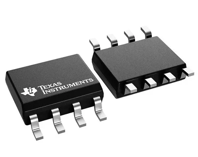

INA122U
Brand: Texas Instruments
Texas Instruments INA122U is a power management component designed for Industrial Automation and related applications. In stock at Superb Automation — request a quote for competitive pricing and fast delivery.
Product Specifications
INA122U
Texas Instruments — Power Management & Signal Chain
Product Overview
The INA122U from Texas Instruments is a power management / signal chain IC delivering high efficiency, precision regulation, and robust protection. Texas Instruments (TI) is a global leader in analog ICs, power management solutions, and embedded processors.
Superb Automation partners with leading brands including Qorvo, TI, ADI, XILINX, NVIDIA, Intel, ST, MACOM, Renesas, and Coilcraft to provide complete BOM and supply-chain solutions.
Key Features
- High-efficiency power conversion with low quiescent current
- Wide input voltage range with precision output regulation
- Integrated over-current, over-temperature, and short-circuit protection
- Small footprint packaging for space-constrained designs
- AEC-Q100 qualified options available for automotive applications
- Flexible sequencing and soft-start control
Key Specifications
| Input Voltage | V |
| Output Voltage | V |
| Output Current | A |
| Switching Frequency | kHz |
| Efficiency | % |
| Quiescent Current | µA |
| Topology | — |
| Package | — |
| Operating Temp | °C |
| Protection | — |
Applications
Industrial Automation
Automotive Electronics
Telecom Infrastructure
Server & Data Center Power
Medical Devices
Consumer Electronics
Request Quote — In Stock, 100% New & Original, Full Warranty
INA122U: the single supply micropower amplifier in a 4.9 by 6 mm SOIC
The INA122U is the surface mount member of this family, in an SO-8 body that measures 4.9 by 6 mm and sits on a reflow line without a second process. The electrical behaviour is the family behaviour: 2.2 to 36 V supply, 60 µA quiescent, rail to rail output, gain from 5 to 10,000 with one resistor, 250 µV offset, 3 µV per degree drift. The body is the reason to pick this row, and on a compact battery instrument the 4.9 by 6 mm footprint is the reason the row exists.
The small body has a thermal consequence as well as an area one. A part that dissipates almost nothing does not care about thermal resistance, so the SO-8's lower thermal resistance is irrelevant; what matters is the shorter lead and the smaller loop, which reduce pickup on a high impedance input.
The INA122U rows as the addendum publishes them
| Part class | Single supply micropower instrumentation amplifier |
| Vendor status | ACTIVE, production data |
| Data sheet | SBOS069B |
| Supply range | 2.2 V to 36 V single or dual |
| Quiescent current | 60 µA |
| Output swing | Rail to rail |
| Gain equation | G = 5 + 200 kΩ divided by RG |
| Gain range | 5 to 10,000 V/V |
| Input offset voltage | 250 µV maximum |
| Offset drift | 3 µV per degree maximum |
| Input bias current | 25 nA maximum |
| Input noise | 60 nV per root Hz |
| Body | SOIC, D outline, 8 pins, 4.9 by 6 mm |
| Carrier | Tube row for this string |
| Reel sibling | INA122U/2K5, 2500 pieces |
| Grade sibling | INA122UA, tighter trimmed bin |
| Moisture level | Level 3, 260 degrees, 168 hour floor life |
| Temperature range | Minus 40 to plus 85 degrees |
The SOIC rows in this family carry level 3 moisture sensitivity while the DIP rows carry not applicable, which is a difference that a build transfer from DIP to SOIC creates without anybody noticing. A tube of SO-8 parts at level 3 has the same 168 hour floor life as a reel, and the bake schedule has to be introduced at the same time as the package change.
Board area, decoupling and a 4.9 mm body
In a 4.9 mm body the decoupling capacitor has to be close, and on a two layer board that usually means directly under the part on the other side. At 60 µA the supply current is not the issue; the issue is the impedance of the supply trace at the frequency of the switching regulator that shares the rail. A 100 nF within a few millimetres and a ground plane under the part is the standard arrangement, and the part's small size makes that easy rather than hard.
The gain resistor placement is the second constraint. At a gain of 100 the resistor is about 1.9 kΩ, which is a small part, and at a gain of 1000 it is about 200 Ω. A 0402 resistor within 2 mm of the pins keeps the loop small, and the trace from one RG pin to the resistor and back should not run past the input pins, because the gain node is a high impedance point at high gain.
What the SOIC body means for a battery product
A battery instrument is usually built in a small enclosure with a double sided board, and the surface mount package is the only sensible choice for all of it. A DIP part in that assembly needs holes through a dense board and a hand solder step, and the resulting product is larger and less reliable than it needs to be. Moving from the DIP to the SOIC is a board change and not a circuit change, which is why the family exists in both bodies.
The other battery consideration is leakage. A 60 µA amplifier in a sealed enclosure with a lithium cell is a build that lasts; the same circuit in a socketed package collects moisture at the socket and the leakage becomes comparable with the supply current. The surface mount part has no socket, which is a reliability argument rather than an electrical one, and it is the argument that matters after the first field failure.
Gain, bandwidth and the 5 V rail
On a 5 V rail with a mid rail reference the part has 2.5 V of output swing in each direction, and the bandwidth at a gain of 100 is set by the two op amp topology rather than by the resistor. A 60 nV per root Hz noise floor at a gain of 100 gives 6 µV per root Hz referred to the input, which on a 1 mV full scale is a signal to noise ratio of about 44 dB in a 1 Hz bandwidth. That is enough for a load cell and not enough for a microphone, which is the boundary of the part's usefulness.
The gain resistor also sets the input impedance seen by the source in some configurations, and a two op amp topology has a signal path through the feedback network that a three op amp part does not. The vendor application circuits are the reference for the input impedance, and a high impedance source should be checked against them before the circuit is committed.
Buying INA122U
The tube row is active and the reel sibling is active. A small build takes the tube, a production build takes the reel, and the difference is only the carrier. The grade decision is between the U and the UA, and on a channel without a trim the A bin is cheap insurance.
The moisture level is the practical difference between this row and the DIP sibling, and a build that has moved from one to the other needs the dry storage procedure in place on day one rather than after the first popcorn failure. Our supplier quality audit page covers what we check at an assembly house on moisture control, and the pin to pin cross reference page lists the bodies we can move between without a circuit change.
Using the part behind a thermocouple
A thermocouple produces tens of microvolts per degree and has a source impedance of a few ohms, so the 25 nA bias current is irrelevant and the 60 nV per root Hz noise is the limiting term. At a gain of 200 a 5 mV full scale becomes 1 V, and the amplifier noise in a 10 Hz bandwidth is about 27 µV referred to the input, which is roughly 0.5 degrees of a type K junction. That is adequate for a process measurement and not adequate for a calibration reference.
The cold junction compensation is a separate channel, and on this part it is often the second amplifier in the same package family, measuring the connector temperature with a thermistor. The two channels then have different gains and different offsets, and the compensation accuracy is set by the thermistor rather than by the amplifier.
The gain resistor for a thermocouple channel is usually a fixed metal film part rather than a trim, because the calibration is done in software against the cold junction. That removes the resistor tolerance from the production test and leaves it in the software constant, which is the pragmatic division of labour on a channel that has to be calibrated per unit anyway.
Questions that arrive with this part number
Whether the SOIC and the DIP are the same circuit is the first question, and they are: same die, same eight pin function assignment, different footprint. Whether the part can run from a single 3 V coin cell is the second, and the supply range allows it, but the cell's internal resistance rises as it discharges and the output current available near the rail falls with it. The third question is the reference: a divider across the cell moves as the cell discharges, so a ratiometric measurement is the only way to use it without a reference.
The fourth is about the missing shutdown pin, which is the same answer as for the DIP row: the supply has to be switched externally if the instrument has to sleep.