


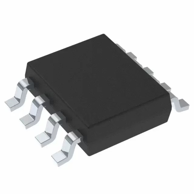

CD4023BE
Brand: Texas Instruments
Texas Instruments CD4023BE is a power management component designed for Industrial Automation and related applications. In stock at Superb Automation — request a quote for competitive pricing and fast delivery.
Product Specifications
CD4023BE
Texas Instruments — Power Management & Signal Chain
Product Overview
The CD4023BE from Texas Instruments is a power management / signal chain IC delivering high efficiency, precision regulation, and robust protection. Texas Instruments (TI) is a global leader in analog ICs, power management solutions, and embedded processors.
Superb Automation partners with leading brands including Qorvo, TI, ADI, XILINX, NVIDIA, Intel, ST, MACOM, Renesas, and Coilcraft to provide complete BOM and supply-chain solutions.
Key Features
- High-efficiency power conversion with low quiescent current
- Wide input voltage range with precision output regulation
- Integrated over-current, over-temperature, and short-circuit protection
- Small footprint packaging for space-constrained designs
- AEC-Q100 qualified options available for automotive applications
- Flexible sequencing and soft-start control
Key Specifications
| Input Voltage | V |
| Output Voltage | V |
| Output Current | A |
| Switching Frequency | kHz |
| Efficiency | % |
| Quiescent Current | µA |
| Topology | — |
| Package | — |
| Operating Temp | °C |
| Protection | — |
Applications
Industrial Automation
Automotive Electronics
Telecom Infrastructure
Server & Data Center Power
Medical Devices
Consumer Electronics
Request Quote — In Stock, 100% New & Original, Full Warranty
CD4023BE: three 3-input NAND gates in a 14-lead plastic DIP
CD4023BE is the triple 3-input NAND of the CD4000B family, three independent gates in a 14-lead plastic DIP, 25 pieces to a tube. The vendor descriptor reads three channels, three inputs, 3 V to 18 V NAND gate, and the document is SCHS021D revision D, which covers the CD4011B, the CD4012B and the CD4023B together. The propagation figure is 60 ns typical at 10 V into a 50 pF load, the same as the rest of the gate family, and the parametric table gives three channels, three inputs per channel, standard CMOS inputs and push pull outputs.
The addendum lists CD4023BE as Active in production, PDIP (N) with 14 leads, 25 pieces to a tube, RoHS yes with a nickel-palladium-gold finish, no moisture level for the through-hole body, minus 55 to plus 125 degrees, and the marking CD4023BE. The same document carries CD4023BM as an obsolete SOIC tube row, CD4023BM96 as the active SOIC reel at 2500 pieces, CD4023BNSR and CD4023BPWR as active 2000 piece reels, and the obsolete BMT row, so the die travels in the same bodies as the CD4011B.
The CD4023BE row as the vendor addendum publishes it
| Part class | Triple 3-input NAND gate, buffered inputs and outputs |
| Vendor descriptor | Three channels, three inputs, 3 V to 18 V NAND |
| Vendor document | SCHS021D revision D, CD4011B, CD4012B and CD4023B |
| Supply range | 3 V to 18 V |
| Parametric ratings | 5 V, 10 V and 15 V tables |
| Propagation delay, vendor figure | 60 ns typical at 10 V into a 50 pF load |
| Output drive, parametric table | 1.5 mA sink and source |
| Output drive, sibling CD4011B table | 6.8 mA sink and source |
| Input current, maximum | 1 microamp at 18 V over the full range, 100 nA at 25 degrees |
| Quiescent current | Tested to maximum at 20 V on every unit |
| Noise margin | 1 V at 5 V, 2 V at 10 V, 2.5 V at 15 V |
| Package for this code | PDIP (N), 14 leads |
| Packing | 25 pieces in a tube |
| Lead finish | NIPDAU |
| Moisture level | Not applicable for this package type |
| Operating range | Minus 55 to plus 125 degrees |
| Status | Active, production |
| Part marking | CD4023BE |
| SOIC rows | CD4023BM Obsolete, CD4023BM96 Active at 2500 pieces |
| SOP and TSSOP members | CD4023BNSR and CD4023BPWR, 2000 piece reels |
| Obsolete row of the same body | CD4023BMT, quantity blank, Call TI |
The drive figure that does not match its own document
The parametric table lists 1.5 mA sink and source for the CD4023B, while the CD4011B, which shares the same document and the same process, lists 6.8 mA. Both figures are printed by the vendor, and this page states both rather than picking the friendlier one. The practical consequence is that a load sized from the 4011 figure can be four times too heavy for a 4023 output, and an output that is asked for more current than the part can give does not simply drop a little: its level collapses towards the rail, and the gate behind it reads the wrong state.
Until the direct current table in the scanned document is read at the rail in question, the safe working assumption is the 1.5 mA figure. That is enough to drive three CMOS inputs, a 10 k load or a small transistor base, and it is not enough to drive an LED at full brightness or a 50 ohm line. A board that needs the gate to drive a load takes the 4011 or adds a transistor.
Where three inputs are the point
A 3-input NAND is the natural element for a glitch free enable: three conditions must all be true before the output goes low, and the output is the inverse of the AND of the three. That is the structure of a safety interlock, of a power sequencing term, and of a chip select that needs an address and a strobe together. Building it from 2-input NANDs costs two gates and an inverter, or two gates if the inverted output is acceptable, so the 4023 saves a package on a board that needs three such terms.
The second use is the oscillator. Three NAND gates with an RC network make a ring oscillator that runs from a few hertz to a few hundred kilohertz depending on the values, and the 4023 gives exactly three gates in one body for the purpose. The frequency stability of that circuit is poor by any modern standard, which is why it survives mainly in blinkers, beepers and test jigs rather than in anything that has to keep time.
Unused inputs, and the way a 3-input gate fails
Every input on a CMOS gate is a gate oxide, and an input that sits at half the rail turns both transistors partly on. On a 3-input part there are nine inputs to account for, and a board that ties two of the three inputs of an unused gate to a rail and leaves the third floating draws current and can oscillate. The rule is that every input on the package goes somewhere, even on an unused gate.
The way this part fails in the field is usually a single input, not the whole gate. A cold joint on one of the three inputs leaves that input floating, and the gate then behaves as a 2-input function of the other two with a random third term, which produces an intermittent fault that changes with temperature and with the state of neighbouring traces. An incoming test that toggles each input separately catches it; a test that applies all three at once does not.
Where the 4023 sits against the 4011 and the 4012
The document covers three widths: four 2-input gates in the CD4011B, two 4-input gates in the CD4012B, and three 3-input gates in the CD4023B. All three carry the same 60 ns typical delay, the same 3 V to 18 V range and the same buffered outputs, and the choice between them is a count of terms. A board with three 3-input terms takes this part; a board with four 2-input terms takes the 4011; a board with two 4-input terms takes the 4012.
Mixing them is normal and usually cheaper than cascading. Each extra gate stage adds 60 ns and one more package to the bill, so a board that needs one wide term and several narrow ones takes one 4012 and one 4011 rather than building the wide term from narrow gates.
Incoming checks and the marking question
The functional test is three rows per gate with each input toggled in turn, at the rail the board uses. The marking should read CD4023BE for the plastic DIP, and the obsolete BMT row of the SOIC body is worth knowing because old stock carries the same die marking as the active row. A drive check at the rail in question, with a load close to the 1.5 mA figure, catches an output stage that has been damaged by an earlier overcurrent event.
The reference pages are the incoming inspection plan, the pin to pin cross reference for the 4011 against 4023 question, and date code management for the traceability rule.
Questions that come up on the 4023
Whether the part can replace a 4011 in a socket. It cannot, because the pinout of a 3-input gate is not the pinout of a 2-input gate, even though both are 14-lead bodies.
Whether two of the three inputs can be tied together to make a 2-input gate. They can, and the result is a 2-input NAND with the delay of the 3-input part, which is the usual way to use a spare gate.
Whether the 1.5 mA drive is a printing error. It is printed in the vendor parametric table and this page does not assume an error; the direct current table in the document is the authority, and until it is read at the rail in question the lower figure is the safe one.
Whether the part is suitable for a battery product. It is, because the static current is in the microamp range and the quiescent current is tested to maximum at 20 V, but the 3 V floor of the supply range sets the end of discharge point for the cell stack.