


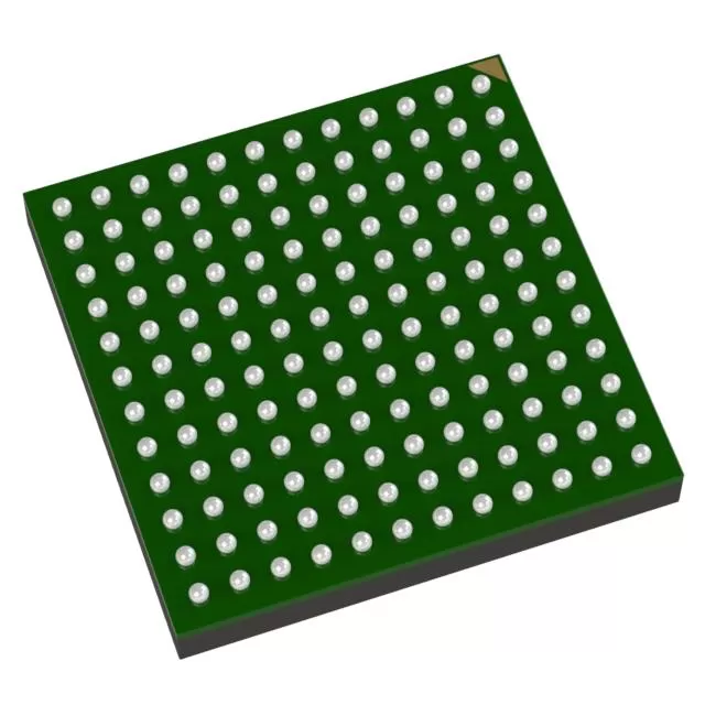

AD9970BCPZRL7
Brand: Analog Devices
Analog Devices AD9970BCPZRL7 is a analog & mixed-signal component designed for Precision Instrumentation and related applications. In stock at Superb Automation — request a quote for competitive pricing and fast delivery.
Product Specifications
AD9970BCPZRL7
Analog Devices — Analog & Mixed-Signal ICs
Product Overview
The AD9970BCPZRL7 from Analog Devices is a high-performance analog / mixed-signal IC providing precision signal acquisition, conversion, and conditioning. Analog Devices (ADI) is a world leader in high-performance analog, mixed-signal, and DSP ICs for instrumentation, healthcare, automotive, and communications.
Superb Automation partners with leading brands including Qorvo, TI, ADI, XILINX, NVIDIA, Intel, ST, MACOM, Renesas, and Coilcraft to provide complete BOM and supply-chain solutions.
Key Features
- High-resolution data conversion with excellent SNR and THD
- Wide dynamic range and high linearity across operating conditions
- Integrated voltage reference with low temperature drift
- Flexible digital interface — SPI, I2C, or parallel options
- Industrial/automotive temperature range with guaranteed specs
- Low power consumption with power-down modes
Key Specifications
| Resolution | bits |
| Channels | — |
| Sample Rate | kSPS |
| Interface | — |
| Supply Voltage | V |
| Operating Temp | °C |
| Package | — |
| INL | LSB |
| SNR | dB |
| THD | dB |
Applications
Precision Instrumentation
Industrial Process Control
Medical Imaging & Diagnostics
Automotive Sensor Interfaces
Communications Infrastructure
Test & Measurement
AD9970BCPZRL7: a 14 Bit CCD Signal Processor Running at 65 MHz
What this part is
The AD9970 is an analogue front end for charge coupled device image sensors: a correlated double sampler, a variable gain amplifier, a 14 bit converter running at 65 megapixels per second, a black level clamp and a complete timing generator with 240 picoseconds of edge resolution, all in a 5 mm by 5 mm 32 lead LFCSP. The timing core drives the sensor clocks directly, with on chip 3 V drivers for the reset gate and the horizontal clock, and the data leaves over a reduced range low voltage differential signalling interface.
The part runs from a 1.8 V analogue and digital core supply, is programmed over a three wire serial port, and is specified from minus 25 to plus 85 degrees C, which is a consumer camera range rather than an industrial one. The vendor marks it as not recommended for new designs, which is the honest starting point for anyone finding this order code on a bill of materials: the function is real and the parts exist, but a new camera board belongs on a current device.
Published figures that matter to a buyer
| Converter | 14 bit, 65 megasamples per second |
| Correlated double sampler | minus 3 dB, 0 dB, plus 3 dB, plus 6 dB |
| Variable gain amplifier | 6 dB to 42 dB, 10 bit control |
| Timing resolution | 240 picoseconds at 65 MHz |
| Black level | clamp with variable level control |
| Clock drivers | 3 V horizontal and reset gate drivers on chip |
| Output interface | reduced range low voltage differential signalling |
| Core supply | 1.8 V analogue and digital |
| Control | 3 wire serial |
| Temperature | minus 25 to plus 85 degrees C |
| Body | 32 lead LFCSP of 5 mm by 5 mm |
| Lifecycle | not recommended for new designs |
Where the headline numbers stop
Two hundred and forty picoseconds sounds like a very fine step until it is put against the clock it is stepping. At 65 megahertz the pixel period is 15.38 nanoseconds, so 240 picoseconds is 1.56 percent of a pixel, and a timing adjustment of one step moves the sample point by that fraction. That is the resolution needed to place a correlated double sample on a sensor whose output settles in a few nanoseconds, and it is the reason the timing generator is on the same die as the sampler: a clock routed across a board would not hold that alignment.
The converter produces 910 megabits per second of raw data at 65 megasamples and 14 bits, which is why the output is differential and why the interface is described as reduced range: the swing is small to keep the edges fast without radiating. On the analogue side, the variable gain amplifier spans 6 dB to 42 dB, which is 63 times of gain range, and the correlated double sampler adds four fixed steps. Between them they set the exposure range the camera can cover, and the 14 bit converter has to hold that whole range without the gain step showing in the image.
Two limits decide whether this part can be used at all in a given build. The temperature range starts at minus 25 degrees C, so an outdoor or industrial camera that must start at minus 40 is outside the specification, and the part is marked as not recommended for new designs, so the supply is broker stock with the traceability and the date code questions that implies. Neither limit makes the part unusable in an existing product; both make it unsuitable for a new one.
Applications where it fits
- Existing professional camcorder and broadcast camera platforms that already carry this order code.
- High end digital still cameras and industrial high speed cameras in service.
- High speed data acquisition front ends built around a charge coupled device sensor.
- Repair and last time buy for camera lines that are still shipping in small volume.
- Test fixtures that emulate a camera front end for a sensor that is still in production.
Two questions buyers ask
Can this drive any charge coupled device sensor? It provides the timing core and the clock drivers for the reset gate, the horizontal clock and the four vertical phases, so the sensor has to be compatible with those outputs and with the 65 megapixel per second rate. A sensor that needs more phases or a faster pixel clock needs a different front end, and the timing program is sensor specific rather than generic.
What replaces it on a new board? That is a system question, because the current generation of camera front ends moves to complementary metal oxide semiconductor sensors with integrated converters. A new build should treat the whole sensor and front end pair as the thing being replaced, and the isolate can only confirm what this part does, not what should take its place.
Sourcing notes and next step
AD9970BCPZRL7 is the 32 lead LFCSP in tape and reel, and the same die appears under two other order codes with different packing. The not recommended for new designs status means the buy is a last time buy or a broker buy, and for a camera line in service the practical answer is a dated stock position rather than a substitution. The analog and mixed signal IC family page lists the converter line, the obsolete part cross reference page sets out how an end of life part is carried, and the BOM shortage recovery page covers the route when the only stock left is distribution remainder.
AD9970BCPZRL7 at 65 megapixels: 910 Mb/s on the link, 240 ps of timing, and a bill of materials that has to plan an end of life
The converter runs at 65 megasamples per second at 14 bits, so the payload on the output is 910 Mb/s and a framed link with a start bit and a stop bit per sample is 975 Mb/s. That is the number that decides whether the receiving end needs one lane or two, and it is worth checking against the receiver before the sensor is chosen: a two lane receiver at 500 Mb/s per lane is comfortable, a single lane at 1 Gb/s is at the edge of what a low cost field programmable gate array input can take without an oversampling clock. The device page states the interface as reduced range low voltage differential signalling, which is a lower swing than standard and is what makes the rate reachable on a small board.
240 ps of edge placement at a 15.4 ns pixel
A 65 MHz pixel period is 15.4 ns, so 240 ps of timing resolution is 1.6 percent of a pixel. That resolution is what allows the reset gate and the horizontal clock to be placed to compensate for the sensor's own delays, and it matters most at the far end of a long horizontal register, where the clock arrives late and the sampling point has to move with it. A camera that shows a shading gradient across the frame at high pixel rates is usually a timing placement problem and not an optical one, and it is fixed in the timing registers rather than with a lens.
Gain range, and what 36 dB means in codes
The variable gain amplifier spans 6 to 42 dB under 10 bit control, which is a 36 dB range, or a factor of 63 in amplitude. The correlated double sampler adds minus 3, 0, plus 3 or plus 6 dB. Taking the lowest and highest ends, the total range is 45 dB, a factor of 178, and at 14 bits the converter has 16,384 codes, so most of that range is used to bring a dim scene up to full scale rather than to extend the dynamic range. A buyer should expect the noise floor to rise with the gain setting, and the point where the analog gain stops helping is where the sensor's own noise exceeds the converter's.
The lifecycle line on the page is the purchasing instruction
The vendor marks this order code as not recommended for new designs. The function is real, the parts exist and they are buyable, and an existing camera that needs a replacement can use them. A new board belongs on a current device. For a programme that has to keep an existing camera in service, the useful exercise is to take the annual volume, multiply by the years of support, and buy to that number while the part is available, because a last time buy is a one time opportunity and a broker purchase afterwards carries a much higher risk of a remarked or out of date part. That arithmetic is a purchasing decision, not an engineering one, and it is better made a year early than a month late.
| Pixel rate | Payload at 14 bits | With framing per sample | Pixel period | 240 ps as a fraction of the pixel |
|---|---|---|---|---|
| 65 MSPS | 910 Mb/s | 975 Mb/s | 15.4 ns | 1.56 percent |
| 40 MSPS | 560 Mb/s | 600 Mb/s | 25.0 ns | 0.96 percent |
| 20 MSPS | 280 Mb/s | 300 Mb/s | 50.0 ns | 0.48 percent |
End of life planning for a camera platform is on component obsolescence management, cross reference work for an obsolete front end is on obsolete part cross reference hub, and the instrument side of the same problem is on medical device components.
Request Quote — In Stock, 100% New & Original, Full Warranty