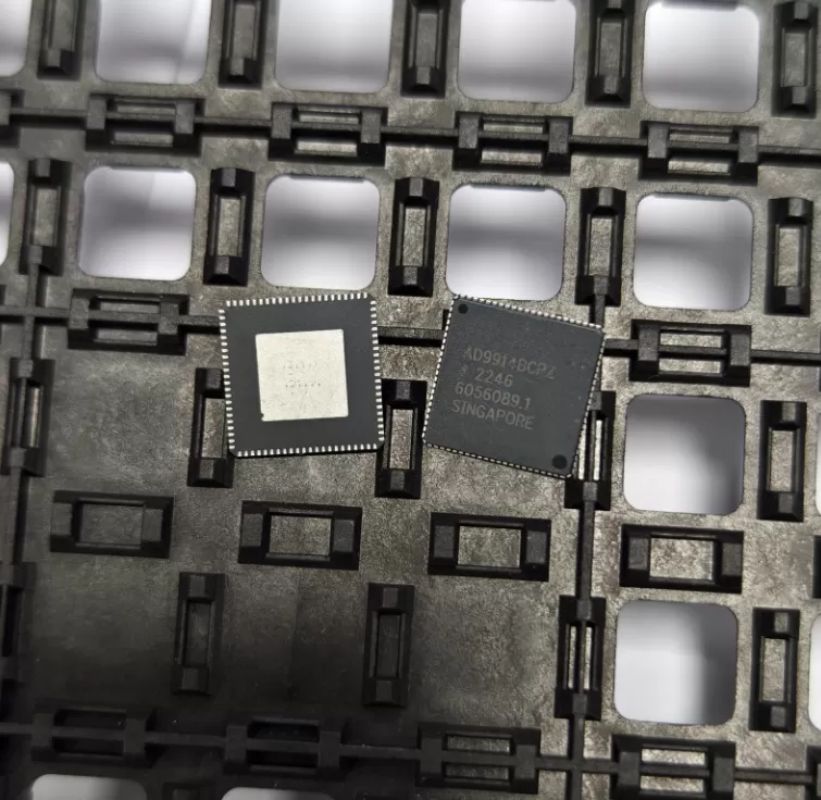
TPS54625PWPR
Brand: Texas Instruments
Texas Instruments TPS54625PWPR is a power management component designed for AI Servers & Low-Altitude Economy (Drone and UAV) and related applications. In stock at Superb Automation — request a quote for competitive pricing and fast delivery.
Product Specifications
TPS54625PWPR
Texas Instruments — Power Management & Signal Chain
Product Overview
The TPS54625PWPR from Texas Instruments is a power management / signal chain IC delivering high efficiency, precision regulation, and robust protection. Texas Instruments (TI) is a global leader in analog ICs, power management solutions, and embedded processors.
Superb Automation partners with leading brands including Qorvo, TI, ADI, XILINX, NVIDIA, Intel, ST, MACOM, Renesas, and Coilcraft to provide complete BOM and supply-chain solutions.
Key Features
- High-efficiency power conversion with low quiescent current
- Wide input voltage range with precision output regulation
- Integrated over-current, over-temperature, and short-circuit protection
- Small footprint packaging for space-constrained designs
- AEC-Q100 qualified options available for automotive applications
- Flexible sequencing and soft-start control
Key Specifications
| Input Voltage | V |
| Output Voltage | V |
| Output Current | A |
| Switching Frequency | kHz |
| Efficiency | % |
| Quiescent Current | µA |
| Topology | — |
| Package | — |
| Operating Temp | °C |
| Protection | — |
Applications
Industrial Automation
Automotive Electronics
Telecom Infrastructure
Server & Data Center Power
Medical Devices
Consumer Electronics
Request Quote — In Stock, 100% New & Original, Full Warranty
TPS54625PWPR: a 6.5 A synchronous buck converter that takes 4.5 V to 18 V in and holds a 0.76 V to 5.5 V rail at a fixed 650 kHz with no external compensation
TPS54625PWPR is a converter with both FETs on the die, an adaptive on-time loop that is stable into ceramic or polymer output capacitors, an adjustable soft start that respects a pre-biased output, and a cycle by cycle current limit in a HTSSOP body of 14 pins. The PWP body is fourteen pins with a PowerPAD on the underside, and the part exists so a 12 V rail can be brought down to a processor rail with one inductor and two capacitors.
Order code and package
| Catalogue string | TPS54625PWPR, where PWP is the fourteen pin HTSSOP with a thermal pad and R is the large tape and reel |
| Body | HTSSOP, PWP, fourteen pins with an exposed PowerPAD that has to be soldered to the plane for the 40.5 C per watt figure to mean anything |
| Reel | 2000 pieces on a large tape and reel, against 90 pieces in a tube on the plain row |
| Finish and moisture | NIPDAU plating, level 2 at 260 C, one year of floor life after the bag is opened |
| Temperature | minus 40 to 85 C free air temperature, so the 6.5 A rating assumes the pad is soldered and the board is not in a hot corner |
| Marking | PS54625 on the body |
| Document | SLVSC33A, August 2013, revised October 2022 |
| Status | Active and in production on the addendum dated November 2025 |
Electrical parameters that decide the application
| Input range | 4.5 V to 18 V, which covers a 5 V rail, a 12 V rail and a 15 V rail with tolerance, and does not cover a 24 V bus |
| Output | 0.76 V to 5.5 V adjustable, with a 753 to 777 mV feedback threshold at 25 C and a 0.765 V nominal used for the soft start arithmetic |
| Current | 6.5 A continuous, with a cycle by cycle limit of 7.2 to 9.5 A measured into a 1.5 uH inductor |
| Switching frequency | fixed 650 kHz, with 150 ns of on time at 12 V in and 1.05 V out and a minimum off time of 260 to 310 ns |
| Switch resistances | 36 mOhm on the high side and 28 mOhm on the low side, which is the conduction loss at 6.5 A |
| Feedback current | 0.02 uA typical and 0.15 uA maximum, so a divider in the hundreds of kilo ohms is allowed |
| Soft start | an external capacitor charged with 4.2 to 7.8 uA, giving a time of the capacitance in nanofarads times 0.84 divided by 6, so 10 nF is about 1.4 ms and 100 nF is about 14 ms |
| Pre-bias | the low side gate pulses start narrow and widen, so a rail that is already up is not pulled down at the start of a sequence |
| Protection | overvoltage at 120 to 130 per cent of the reference with a 10 us response, undervoltage at 60 to 70 per cent with 10 per cent of hysteresis and a 0.25 ms delay, and thermal shutdown at 165 C |
| Undervoltage lockout | 3.45 to 4.05 V on the internal VREG5 rail with 0.13 to 0.48 V of hysteresis, which is a higher threshold than the 4.5 V input floor |
| Power good | an open drain output that asserts above 85 to 95 per cent of the reference and de-asserts at 85 per cent falling |
| Shutdown | under 10 uA with the enable low, and the internal discharge path is not present, so the output decays into the load |
Where the part fits against a module or a controller
| TPS54625PWPR | fourteen pin HTSSOP, 2000 pieces on a large reel, this page |
| TPS54625PWP | the same die in a 90 piece tube, which is the row a prototype order uses and the row that is easiest to lose in goods inwards |
| A converter with a higher input | a 24 V bus needs a part rated above 18 V, and the 18 V ceiling here is a silicon limit rather than a marketing figure |
| A converter with a lower current | a 3 A part in the same family drops into a smaller body and a smaller inductor, and the soft start arithmetic is the same |
| A module with the inductor inside | a module removes the inductor and the loop from the bill of materials and costs board area with a fixed height |
| A controller with external FETs | a controller moves the heat off the package and adds two FETs, a driver and a loop that has to be measured |
Points to check before this part goes on a BOM
The pre-biased start is the feature that matters on a multi rail board. When a processor rail is sequenced after an input output rail, the output capacitor can be sitting at a volt before the converter is enabled, and a converter that pulls the rail down to zero before ramping it up disturbs everything downstream. Here the low side gate pulses start narrow and widen cycle by cycle until the duty cycle matches the operating point, so the output starts from wherever it is and rises. That behaviour has to be tested with a real pre-bias, not assumed from the feature list.
The current limit is measured into a 1.5 uH inductor and the number moves with the inductor. At 650 kHz and 12 V in, 1.5 uH carries about 1.4 A of ripple, so a 7.2 A minimum limit is 5.8 A of average current plus the ripple peak. Change the inductor to 1 uH and the ripple rises to 2.1 A, the peak arrives sooner, and the average current at which the limit trips falls. A board that needs the full 6.5 A has to keep the inductor at or above 1.5 uH and check the limit at the highest input voltage.
The undervoltage lockout sits on the internal 5 V regulator and not on the input. It releases between 3.45 and 4.05 V of VREG5, so the converter starts well below its 4.5 V input floor and then the loop has to cope with a very low input, which it does by running at the maximum duty cycle. The practical consequence is that a slow input ramp produces output before the input is in its specified range, and a board that needs a clean start should hold the enable off until the input is above 4.5 V rather than rely on the lockout.
Thermal performance is entirely a function of the PowerPAD. The 40.5 C per watt junction to ambient figure assumes the pad is soldered to a plane with vias, and 6.5 A at 36 and 28 mOhm dissipates about 1.1 W in the FETs plus 0.1 W in the controller. At 40.5 C per watt that is 49 C of rise, so a 60 C ambient takes the junction to 109 C and a 85 C ambient takes it past the limit. A board that runs at full current in a hot enclosure needs either a lower input voltage, a lower current or a bigger copper area under the pad.
The 18 V input ceiling is the boundary to watch on an industrial board. A 12 V rail with a 20 per cent tolerance reaches 14.4 V and is fine, and a 15 V rail reaches 18 V and is at the limit with no margin for a transient. A 24 V bus is outside the rating entirely and the part will not survive a hot plug event on that bus, whatever the absolute maximum table says. The next part up in the family covers 28 V and is the honest choice for a 24 V bus.
The feedback threshold at 753 to 777 mV is a plus or minus 1.5 per cent window at 25 C, and the divider tolerance adds to it. A 1.0 V rail built from a 1 per cent divider and this window lands inside plus or minus 2.5 per cent, which is usually acceptable for a processor core and not acceptable for an analog rail. A board that needs a tight rail should check whether the fixed voltage members of the family, or a converter with a tighter reference, do a better job than a divider on this part.
Working the soft start back from the load
The soft start capacitor is charged with 6 uA and the ramp is complete when the feedback reaches 0.84 V, so the time in milliseconds is the capacitance in nanofarads times 0.84 divided by 6. A 10 nF capacitor gives 1.4 ms, a 47 nF capacitor gives 6.6 ms and a 100 nF capacitor gives 14 ms. The number that matters is the inrush into the output capacitance: 470 uF charged to 1.0 V in 1.4 ms draws 336 mA on top of the load, and in 14 ms it draws 34 mA.
A pre-biased output changes the arithmetic rather than the capacitor. If the output starts at 0.5 V and has to reach 1.0 V, the ramp only covers half the range and the inrush is halved, but the converter has to survive the initial condition without pulling the rail down. Test it with the pre-bias present on the bench, because a board that starts clean into a discharged capacitor can still dip when the capacitor is already charged.
Reading the current limit against a real inductor
The limit is a peak comparator, so the average current at which it trips is the limit minus half the ripple. At 12 V in, 1.0 V out and 650 kHz with a 1.5 uH inductor, the ripple is 1.4 A and the average trip is between 6.5 A and 8.8 A. At 18 V in the ripple rises to 2.1 A and the average trip falls to between 6.2 A and 8.5 A. That is the range a board actually sees, and it is why a 6.5 A rating is not a 9.5 A margin.
Saturation is the other half. The inductor has to hold its value at the trip current, not at the rated current, because the limit is a peak and the peak is above the average. A 6.5 A inductor with a 20 per cent drop at 7.8 A is at the edge of a 9.5 A maximum limit, and a fault that pushes the current to the limit will take it into saturation and turn a current limit into a short circuit.
Where this order code fits
This is the 12 V to core or 12 V to 5 V stage in a set top box, a digital television, a network appliance, a disk enclosure or an industrial controller, where a single inductor and two ceramic capacitors have to carry 6.5 A at 650 kHz without a compensation network Teams comparing it with a neighbouring part start from our Power Management Cross Reference page, and teams replacing a part that has gone end of life start from the Component Lead Time Solutions page.
Questions buyers ask
Does it need external compensation? No. The adaptive on-time loop is stable into ceramic or polymer output capacitors and there is no compensation pin.
What is the current limit? Peak detection between 7.2 A and 9.5 A measured into a 1.5 uH inductor, so the average trip is lower by half the ripple, which is 0.7 A at 12 V in.
Can the output start with a pre-bias? Yes. The low side pulses start narrow and widen, so a charged output is not pulled down before the ramp begins.
Is 18 V input enough for a 24 V bus? No. 18 V is the operating maximum and a 24 V bus exceeds it even before a transient. The family part rated to 28 V is the right choice for that bus.
Why does the lockout release below the input floor? The lockout watches the internal 5 V regulator at 3.45 to 4.05 V, so the converter can start before the input reaches 4.5 V. Hold the enable off until the input is in range if a clean start matters.
SUPERB holds and sources this line for production and repair demand, quoted against the exact ordering string with date codes, packing and country of origin stated on the offer. When a part is moving, the Pin to Pin Cross Reference page sets out the checks that keep a substitute from failing on the bench.