


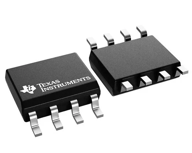

OPA356AID
Brand: Texas Instruments
Texas Instruments OPA356AID is a power management component designed for Industrial Automation and related applications. In stock at Superb Automation — request a quote for competitive pricing and fast delivery.
Product Specifications
OPA356AID
Texas Instruments — Power Management & Signal Chain
Product Overview
The OPA356AID from Texas Instruments is a power management / signal chain IC delivering high efficiency, precision regulation, and robust protection. Texas Instruments (TI) is a global leader in analog ICs, power management solutions, and embedded processors.
Superb Automation partners with leading brands including Qorvo, TI, ADI, XILINX, NVIDIA, Intel, ST, MACOM, Renesas, and Coilcraft to provide complete BOM and supply-chain solutions.
Key Features
- High-efficiency power conversion with low quiescent current
- Wide input voltage range with precision output regulation
- Integrated over-current, over-temperature, and short-circuit protection
- Small footprint packaging for space-constrained designs
- AEC-Q100 qualified options available for automotive applications
- Flexible sequencing and soft-start control
Key Specifications
| Input Voltage | V |
| Output Voltage | V |
| Output Current | A |
| Switching Frequency | kHz |
| Efficiency | % |
| Quiescent Current | µA |
| Topology | — |
| Package | — |
| Operating Temp | °C |
| Protection | — |
Applications
Industrial Automation
Automotive Electronics
Telecom Infrastructure
Server & Data Center Power
Medical Devices
Consumer Electronics
Request Quote — In Stock, 100% New & Original, Full Warranty
OPA356AID: 200 MHz CMOS voltage-feedback operational amplifier with 360 volts per microsecond in an 8-pin SOIC
OPA356AID is a high speed CMOS voltage-feedback operational amplifier with 360 volts per microsecond of slew, aimed at video and cable driving in a SOIC body of 8 pins. The AID suffix is the 8-pin SOIC body, one of two shapes the A grade is offered in alongside SOT-23-5. The published headline is 450 MHz of unity gain bandwidth and a 200 MHz gain bandwidth product with 360 volts per microsecond of slew, drawing 8.3 milliamps typical and 11 milliamps maximum from a 2.7 V to 5.5 V supply. The table is specified with a 604 ohm feedback resistor and a 150 ohm load returned to mid-supply, which is a cable driver condition rather than a generic one.
Order code and package
| Order code | OPA356AID |
| Function | CMOS voltage-feedback operational amplifier, high speed |
| Package | SOIC, 8 pins, body code D |
| Supply range | 2.7 V to 5.5 V |
| Supply current | 8.3 milliamps typical, 11 milliamps maximum per amplifier |
| Unity gain bandwidth | 450 MHz |
| Gain bandwidth product | 200 MHz |
| Slew rate | 360 volts per microsecond |
| Test condition | 604 ohm feedback, 150 ohm load to mid-supply |
| Input common mode | 100 millivolts below the negative rail to 1.5 V below the positive rail |
| Output | rail to rail, current limited |
| Datasheet | OPAx356, OPA2356 family document |
Electrical parameters that decide the application
| Offset | 2 millivolts typical, 9 millivolts maximum at 5 V, 15 millivolts over temperature |
| Offset drift | 7 microvolts per degree |
| Input bias current | 3 picoamps typical, 50 picoamps maximum |
| Voltage noise | 5.8 nanovolts per root hertz at 1 MHz |
| Current noise | 50 femtoamps per root hertz at 1 MHz |
| Common-mode rejection | 66 dB minimum, 80 dB typical at 5.5 V |
| Open-loop gain | 84 dB minimum, 92 dB typical into 150 ohms |
| Power-supply rejection | 80 microvolts per volt typical, 350 microvolts per volt maximum |
| Input capacitance | 1.5 picofarads differential, 1.5 picofarads common mode |
Points to check before this part goes on a BOM
9 millivolts of maximum offset and 15 millivolts over temperature are a video specification, not a measurement one. On a 12 bit converter at 5 V that is 7.4 to 12 bits of offset, so the part cannot be used anywhere the DC level is the information. In a video path the signal is AC coupled and the offset is stripped by a clamp, which is why the datasheet spends its table on slew rate and settling rather than on offset.
360 volts per microsecond supports a 4 V peak to peak signal to about 14 MHz and a 2 V peak to peak signal to 28 MHz, while the 200 MHz gain bandwidth product allows a 20 MHz signal at a gain of 10. At the top of the video band the slew rate and the gain limit converge, so a board that runs a 1080 line signal at a gain of two uses both together and has little margin for overshoot.
The 150 ohm load condition is the whole thermal story. Driving a 75 ohm cable through a 75 ohm back termination presents 150 ohms, and a 2 V peak to peak signal into that load is 13.3 milliamps peak, which is 13.3 milliwatts. With 11 milliamps of supply current at 5 V already spent inside the package, the output stage current is the same order as the quiescent current, and the SOIC body has to pass both.
50 picoamps of maximum bias current is negligible at any normal source impedance, but the input is not rail to rail. The common mode stops 1.5 V below the positive rail, so on a 5 V supply the ceiling is 3.5 V and a video signal whose sync tip sits at 4.7 V is outside the window. AC coupling with a bias point at 2.5 V is the normal arrangement, and it also keeps the input stage away from the changeover region.
5.8 nanovolts per root hertz at 1 MHz is a respectable noise density for a CMOS input, and at a 150 ohm load the resistor noise of the load itself is 1.6 nanovolts per root hertz, so the amplifier contributes about 3.6 times the thermal noise of the cable termination. In a video path that is irrelevant because the signal to noise is set by the source; in a 10 MHz instrumentation path behind a 50 ohm source the total noise is dominated by the 0.9 nanovolts of the source resistance.
8.3 milliamps typical and 11 milliamps maximum per amplifier means a quad board with four of these draws 44 milliamps into a small area. The 450 MHz figure is small signal at unity gain, and the moment the circuit runs at a gain of five the usable bandwidth drops to about 40 MHz because the gain bandwidth product is 200 MHz, not 450. Quoting the unity gain figure at a gain of five is the most common error in a specification review on this part.
Where this order code fits
Video distribution amplifiers, CCD and CMOS sensor buffers, active filters above 10 MHz and 75 ohm cable drivers use this part. The 150 ohm load test condition is the giveaway: this is an amplifier specified to drive a terminated line, not a high impedance converter input. Boards comparing it with a neighbouring part start from our How to Choose an RF Amplifier page, and boards replacing a part that has gone end of life start from the Amplifier Cross Reference page.
Questions buyers ask
Why does the datasheet test with a 604 ohm feedback resistor? Because the part is specified as a video cable driver, and 604 ohms with a 150 ohm load sets the gain and the loading that a terminated line presents. Numbers taken in a different network are not the published numbers.
Is 450 MHz available at a gain of five? No. 450 MHz is the unity gain bandwidth and the gain bandwidth product is 200 MHz, so a gain of five gives about 40 MHz. The slew rate of 360 volts per microsecond is a separate limit.
Can this part be used for a DC measurement? Only with a wide error budget. The offset is 9 millivolts maximum and 15 millivolts over temperature, which is 7 to 12 bits of a 12 bit converter at 5 V.
SUPERB holds and sources this Texas Instruments line for production and repair demand, quoted against the exact ordering string with date codes, packing and country of origin stated on the offer. When a line is moving, the RF Component Sourcing page sets out the checks that keep a substitute from failing on the bench.