An RF amplifier request usually arrives as two numbers: a frequency band and a gain, or a band and an output power. The first quote then comes back for a device that meets both on the summary page and fails on the board six weeks later, because gain and band are the easiest parameters to compare and the least useful on their own. Choosing an RF amplifier is matching one device to one signal chain, and the parameters that decide the outcome sit further down the datasheet.
The same part can be excellent in a 50 ohm fixture and marginal in the product, because the fixture is matched, cooled and driven with a single tone, while the board has a real load, a real temperature and a modulated signal.
Where an RF amplifier choice goes wrong
Gain without compression point is the first trap. A device with 20 dB of gain and 10 dBm of output at 1 dB compression cannot deliver the level the antenna needs, whatever the gain figure suggests, and the missing decibels are paid for later with a second stage.
Linearity is the second. Third order intercept is quoted at a tone spacing and tone power that may not match the signal in use, and a device that is linear with two small tones can produce spectral regrowth on a modulated carrier.
Noise figure is the third. It has to hold at the band edges and at the match the board presents, not only at the centre frequency in a matched fixture: 0.8 dB at mid band and 1.6 dB at the edge is a different system budget.
Thermal behaviour is the fourth. A power stage at 30 percent efficiency with a modulated signal turns most of its input power into heat, which has to leave through the package, the thermal pad and the copper beneath it. Junction temperature at the enclosure temperature decides whether the part survives the warranty.
Bias comes fifth. GaN and depletion mode parts need a negative gate bias before the drain voltage, and the order has to hold at power up, power down and every brown out. A network that is right on the bench and wrong at a hot restart is a field return.
Then stability outside the band. A device that is stable from 1 to 3 GHz can oscillate at 200 MHz where its gain is higher and the decoupling weaker, and it shows up as a raised noise floor rather than a fault.
The parameters that decide an RF amplifier choice
| Parameter | Why it decides the outcome | What a weak comparison looks like |
|---|---|---|
| Frequency range and band edges | Gain, power and match all fall away at the edges | Centre frequency quoted, edge performance not shown |
| Gain and gain flatness | Sets the budget and the correction the system needs | One gain figure, no flatness across the band |
| Output power at 1 dB compression | Decides the level the chain can hold without compression | Saturated power quoted as if it were linear power |
| Third order intercept | Decides distortion with two or more carriers | Intercept at a different tone spacing and tone power |
| Noise figure | Sets the sensitivity of the receive path | Mid band figure only, edge and match not compared |
| Supply voltage and current | Decides the rail, the budget and the heat | Current at quiescent only, peak current not shown |
| Efficiency at back off | Sets the heat that has to leave the package | Peak efficiency quoted for a backed off signal |
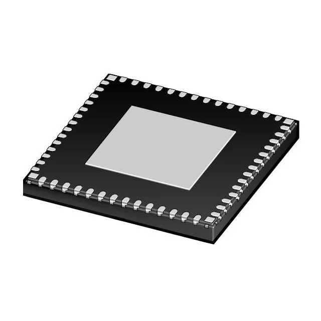
| Package and thermal path | Pad size and thermal resistance decide the copper area | Same pin count, pad and thermal path not compared |
| Bias and sequencing | Gate bias order decides survival at power up and down | Bias network copied from a different device family |
| Grade and lifecycle | Screening, temperature range and remaining life decide risk | Commercial part offered for an outdoor unit |
How SUPERB PCBA supports an RF amplifier choice
Send the band with the modulation, the output power at the antenna port, the gain budget, the rails, the footprint you can accept, the board temperature inside the enclosure and the annual quantity. The reply is a shortlist of two or three devices with the parameters read at the band edges, the derating at your board temperature, and each difference marked as compatible, needs a check, or needs a board change.
Candidate parts are grouped under amplifiers and comparators, and the power stage side of the same chain is covered by the RF power amplifier board family. Where the original device is already end of life, the routes are collected in the amplifier cross reference page, so the shortlist starts from parts that can still be bought next year.
Provenance comes before the sample. Reels are counted by X-ray, markings and date codes are inspected, and decapsulation is used where the risk justifies it. Verified lots carry a 730 day warranty, and a substitution only enters the bill of materials after written approval.
Matching the amplifier to the board rather than the fixture
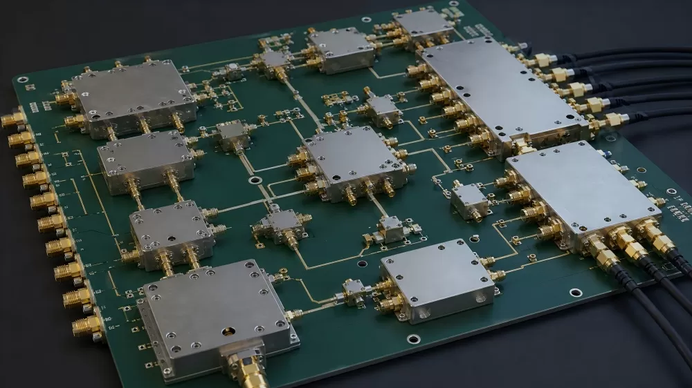
Device and board are qualified together. The input and output match, the bias network, the decoupling and the thermal vias belong to one space, and the measurement that matters is taken at the connector of the assembled board, at the product temperature.
SUPERB Assembly builds and tests that board: first article inspection against released data, 3D SPI before reflow, 3D AOI after it, X-ray in 2D and CT mode with voiding below 5 percent, and functional test on a fixture approved by your team, including gain, return loss and output power at the band edges. The work runs under IPC-A-610 Class 2 and Class 3, ISO 9001, and ISO 13485 for medical programmes, with placement down to 01005, boards supported from 500 MHz to 77 GHz, impedance held to plus or minus 5 percent and to plus or minus 2 percent where the circuit needs it, and up to 68 layers.
RF amplifier questions
Is a higher gain part always the safer choice?
No. Extra gain in one stage usually costs linearity or stability, and it can make the following stage compress earlier. The chain sets the gain budget.
Can a part quoted at a higher output power replace a smaller one?
Only if the bias, the supply current and the thermal path still suit the board. A larger die with the same footprint can need more copper and a different bias network.
How is a drop in replacement proved?
With the parameters compared at the band edges, the bias verified on the assembled board, and gain, return loss and output power measured at the temperature corners. A datasheet match alone proves very little.
What if the replacement needs a different bias voltage?
Then it is a board change and it is quoted as one, with the sequencing, the current limit and the test plan included so the cost is known before the order.
Next step
Send the band with modulation, the required output power, the gain budget, the rails, the footprint you can accept and the annual quantity. You get the shortlist with the parameters at the band edges, the availability of each candidate, and the measurements needed to release the change.