


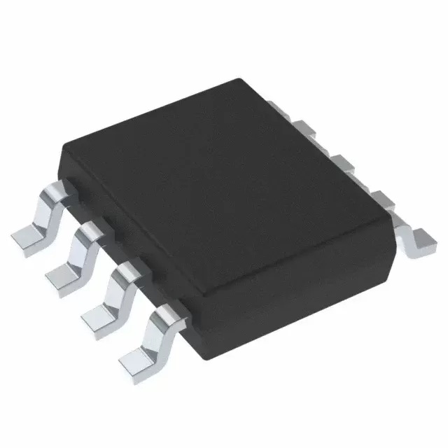

INA818IDR
Brand: Texas Instruments
Texas Instruments INA818IDR is a power management component designed for Industrial Automation and related applications. In stock at Superb Automation — request a quote for competitive pricing and fast delivery.
Product Specifications
INA818IDR
Texas Instruments — Power Management & Signal Chain
Product Overview
The INA818IDR from Texas Instruments is a power management / signal chain IC delivering high efficiency, precision regulation, and robust protection. Texas Instruments (TI) is a global leader in analog ICs, power management solutions, and embedded processors.
Superb Automation partners with leading brands including Qorvo, TI, ADI, XILINX, NVIDIA, Intel, ST, MACOM, Renesas, and Coilcraft to provide complete BOM and supply-chain solutions.
Key Features
- High-efficiency power conversion with low quiescent current
- Wide input voltage range with precision output regulation
- Integrated over-current, over-temperature, and short-circuit protection
- Small footprint packaging for space-constrained designs
- AEC-Q100 qualified options available for automotive applications
- Flexible sequencing and soft-start control
Key Specifications
| Input Voltage | V |
| Output Voltage | V |
| Output Current | A |
| Switching Frequency | kHz |
| Efficiency | % |
| Quiescent Current | µA |
| Topology | — |
| Package | — |
| Operating Temp | °C |
| Protection | — |
Applications
Industrial Automation
Automotive Electronics
Telecom Infrastructure
Server & Data Center Power
Medical Devices
Consumer Electronics
Request Quote — In Stock, 100% New & Original, Full Warranty
INA818IDR: the low power precision front end on a 2500 piece reel
INA818IDR is the precision instrumentation amplifier in the 8 pin SOIC of 4.90 by 3.91 millimetres, on a 2500 piece large reel. It holds 10 microvolts typical and 35 microvolts maximum of offset with 0.4 microvolts per degree of drift, draws 385 microamps maximum, and sets any gain from 1 to 10 000 with one resistor.
The reel is the only carrier this part is offered in, which is a detail worth knowing when a prototype needs a handful: the tube code in the same body is a separate orderable string, and the reel is what a line buys. The input stage is a super beta pair rather than a chopper, so the part has no clock and no switching residue, and the inputs survive 60 volts beyond the rails.
INA818IDR as the vendor document publishes it
| Offset voltage | 10 microvolts typical, 35 microvolts maximum |
| Offset drift | 0.4 microvolts per degree |
| Gain equation | 1 plus 50 kilo-ohms divided by the gain resistor |
| Gain range | 1 to 10 000 V/V |
| Gain error at a gain of 10 | 0.025 per cent typical, 0.15 per cent maximum |
| Gain drift at 1 | 5 ppm per degree maximum |
| Gain drift above 1 | 35 ppm per degree maximum |
| Common mode rejection at a gain of 10 | 110 dB minimum |
| Power supply rejection at a gain of 1 | 100 dB minimum |
| Input bias current | 0.15 nanoamps typical, 0.5 nanoamps maximum |
| Voltage noise | 8 nanovolts per root hertz |
| Bandwidth at a gain of 1 | 2 MHz |
| Bandwidth at a gain of 100 | 270 kHz |
| Stable load capacitance | 1 nanofarad |
| Input protection | 60 volts beyond the supply rails, input current limited to 8 milliamps |
| Supply current | 385 microamps maximum |
| Supply range | 4.5 to 36 volts single, plus or minus 2.25 to plus or minus 18 volts dual |
| Output | rail to rail |
| Temperature range | minus 40 to plus 125 degrees |
| Vendor status | active, 2500 piece large reel |
| Catalogue code | INA818IDR |
| Vendor string | INA818IDR |
| Marking | INA818 |
| Lead finish | NIPDAU |
| Moisture level | level 2, 260 degrees, one year floor life |
Thirty five microvolts from a super beta input stage
The offset of INA818IDR is 10 microvolts typical and 35 microvolts maximum referred to the input, with a drift of 0.4 microvolts per degree. That is a super beta input pair rather than a chopper, so the offset is low without the clock and the settling behaviour of an auto-corrected stage.
The split between the input stage and the output stage is published, and it matters: the input stage carries the 35 microvolts and the output stage carries its own offset, which appears divided by the gain. The two drift terms are uncorrelated, so the input referred drift is the root of the sum of squares rather than a simple addition. A channel at a gain of 100 therefore lives almost entirely on the input stage rows, and the output stage terms fall below the resolution of the measurement.
Eight nanovolts, which is a resistor level noise floor
The voltage noise of INA818IDR is 8 nanovolts per root hertz, which is close to the thermal noise of a 4 kilo-ohm resistor, so a source above a few kilo-ohms is limited by the source rather than by the amplifier. The bias current of 0.15 nanoamps typical and 0.5 maximum turns into 5 microvolts across a 10 kilo-ohm source, which is well under the offset.
The pair of numbers is what makes the part usable on a strain gauge or a low impedance bridge. A 350 ohm bridge has a thermal noise of about 2.4 nanovolts per root hertz, so the amplifier contributes about three times that, and the total is still a fraction of a microvolt across a 10 kilohertz band. On a 1 megohm source the current noise and the bias current take over and the 8 nanovolt figure becomes irrelevant.
Two megahertz at unity gain, and the gain law
The gain of INA818IDR is 1 plus 50 kilo-ohms divided by the resistor between the gain pins, so any gain from 1 to 10 000 comes from one resistor. The 3 dB bandwidth is 2 MHz at unity gain and 270 kHz at a gain of 100, and the part is stable with a 1 nanofarad load, which means a converter's sampling capacitor does not need an isolation resistor.
The gain drift of 5 ppm per degree at unity and 35 ppm per degree above unity is the row that separates the internal network from the external resistor. Above unity, the external resistor sets the drift as well as the accuracy, and a 25 ppm per degree resistor doubles the published figure. At unity the pins are open and the internal network alone sets the channel, which is the only condition where the 5 ppm figure applies.
Sixty volts of input protection, and what it costs
The inputs of INA818IDR survive 60 volts beyond the supply rails by limiting the input current to less than 8 milliamps, which is a real number for an industrial front end that sees a transducer cable unplugged while the rail is up, or a 24 volt field line shorted to a sensor input.
The protection is not free. The series resistance in the input path adds to the source impedance, and its tolerance appears as a gain error on an unbalanced source, so a channel that needs the tightest gain has to keep the source balanced. The protection also sets the maximum input current a fault can deliver, and a 60 volt fault through a 10 kilo-ohm source is 6 milliamps, which is inside the limit; through a 100 ohm source it is 600 milliamps, which is not. The 60 volt figure is a specification of the part with a current limited source, not a licence to connect it to a bus.
A hundred and ten decibels at a gain of ten
The common mode rejection of INA818IDR is 110 dB minimum at a gain of 10, and the rejection at unity gain is quoted separately because the input stage is a different configuration there. The part is built for a high rejection across the full input window, and the data sheet states that the rejection at unity gain exceeds 90 dB over that window.
For an industrial channel that rejection is the reason to buy the part rather than a general purpose amplifier. A 110 dB figure turns a 10 volt common mode into 30 microvolts at the input, which is the same size as the offset and therefore the point where the two error terms are balanced. Below that the offset limits the channel, above it the rejection does, and a channel with a 24 volt common mode on a 5 volt supply is the case the part was made for.
Where a precision low noise front end belongs
INA818IDR belongs on a strain gauge or a load cell, a flow transmitter, a battery test channel, a medical front end that has to hold its offset without a chopper clock, and an industrial input module where a 24 volt field line has to be protected and rejected.
It stops at four things. The supply floor is 4.5 volts single, so a 3.3 volt rail is out. The quiescent current of 385 microamps is fine for a mains instrument and too much for a coin cell. The common mode range is the supply, so a high side shunt on a 48 volt bus needs a different front end. And the offset class of 35 microvolts is right for a millivolt signal and marginal for a thermocouple, where a chopper part is the better answer. Our amplifier cross reference page covers the zero drift alternatives, and the vendor consolidation page covers buying the family on one line.
The offset and the noise are the two rows this part is bought on. Our amplifier cross reference page covers the wider bandwidth member of the family, and the traceability report page covers the certificate that travels with the reel.
Is the 35 microvolt offset measured at the input or the output? At the input, and the output stage offset is a separate row that arrives divided by the gain.
What limits the channel at a gain of 100? The input stage offset of 35 microvolts; the output stage term falls to 8 microvolts at that gain.