


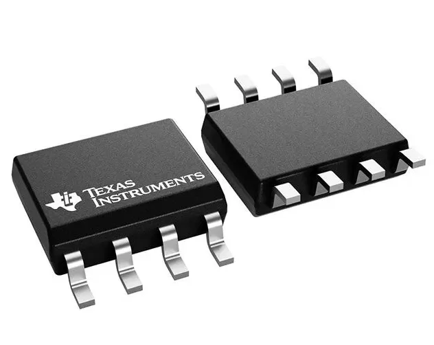

INA186A3IDDFR
Brand: Texas Instruments
Texas Instruments INA186A3IDDFR is a power management component designed for Industrial Automation and related applications. In stock at Superb Automation — request a quote for competitive pricing and fast delivery.
Product Specifications
INA186A3IDDFR
Texas Instruments — Power Management & Signal Chain
Product Overview
The INA186A3IDDFR from Texas Instruments is a power management / signal chain IC delivering high efficiency, precision regulation, and robust protection. Texas Instruments (TI) is a global leader in analog ICs, power management solutions, and embedded processors.
Superb Automation partners with leading brands including Qorvo, TI, ADI, XILINX, NVIDIA, Intel, ST, MACOM, Renesas, and Coilcraft to provide complete BOM and supply-chain solutions.
Key Features
- High-efficiency power conversion with low quiescent current
- Wide input voltage range with precision output regulation
- Integrated over-current, over-temperature, and short-circuit protection
- Small footprint packaging for space-constrained designs
- AEC-Q100 qualified options available for automotive applications
- Flexible sequencing and soft-start control
Key Specifications
| Input Voltage | V |
| Output Voltage | V |
| Output Current | A |
| Switching Frequency | kHz |
| Efficiency | % |
| Quiescent Current | µA |
| Topology | — |
| Package | — |
| Operating Temp | °C |
| Protection | — |
Applications
Industrial Automation
Automotive Electronics
Telecom Infrastructure
Server & Data Center Power
Medical Devices
Consumer Electronics
Request Quote — In Stock, 100% New & Original, Full Warranty
INA186A3IDDFR: the 100 V/V member with both pins on a large reel
INA186A3IDDFR is the 100 V/V member of the current sense family in the eight pin thin body on a 3000 piece large reel. At this gain a 10 milliohm shunt carrying 1 amp produces 100 millivolts at the output, and a 1 milliohm shunt carrying 10 amps produces the same, so the option suits a wide range of low voltage rails without changing the shunt.
The body keeps the reference and the enable pins, which makes this the code for a channel that has to read both directions and sleep between readings. The bandwidth at this gain is 37 kHz, the offset window is 50 microvolts maximum, and the whole part runs from 1.7 volts, which is the row that matters on a 1.8 volt rail with no other supply available.
INA186A3IDDFR as the vendor document publishes it
| Gain | 100 V/V fixed |
| Gain error | 0.04 per cent typical, 1 per cent maximum |
| Gain error drift | 2 ppm per degree typical, 10 maximum |
| Nonlinearity | 0.01 per cent typical of full scale |
| Offset voltage | 3 microvolts typical, 50 microvolts maximum, referred to the input |
| Offset drift | 0.05 microvolts per degree typical, 0.5 maximum |
| Input bias current | 0.5 nanoamps typical, 3 nanoamps maximum |
| Input offset current | 70 picoamps typical |
| Common mode rejection | 120 dB minimum, 150 typical, measured over minus 40 to plus 125 degrees |
| Power supply rejection | 1 microvolt per volt typical, 10 maximum |
| Reference rejection | 0.01 per cent typical, 10 microvolts per volt maximum |
| Common mode range | minus 0.2 volts to plus 40 volts, independent of the supply |
| Supply range | 1.7 volts to 5.5 volts |
| Quiescent current | 48 microamps typical, 65 maximum, 90 over temperature |
| Shutdown current | 10 nanoamps typical, 100 maximum |
| Bandwidth | 45 kHz at 25 V/V, 37 kHz at 100 V/V, 35 kHz at 500 V/V, intermediate options between those |
| Slew rate | 0.3 volts per microsecond |
| Settling to 1 per cent | 30 microseconds from a current step |
| Voltage noise | 75 nanovolts per root hertz |
| Swing to the positive rail | 20 millivolts typical, 40 maximum into 10 kohm |
| Swing to ground | 0.05 millivolts typical, 1 maximum |
| Zero current output | 2 millivolts typical, 10 maximum with the reference grounded |
| Stable load capacitance | 1 nanofarad |
| Temperature range | minus 40 to plus 125 degrees |
| Vendor status | active, 3000 piece large reel |
| Catalogue code | INA186A3IDDFR |
| Vendor string | INA186A3IDDFR |
| Body | SOT-23 thin, DDF, eight pin |
| Moisture level | level 1, 260 degrees, no floor life limit |
| Direction | bidirectional, reference pin available |
One hundred and twenty decibels of rejection against a fixed noise floor
The rejection of INA186A3IDDFR is 120 dB minimum, so a 1 volt swing on a 40 volt common mode becomes 1 microvolt at the input. The voltage noise density is 75 nanovolts per root hertz, so a 10 kHz bandwidth carries 7.5 microvolts of noise and a 1 kHz bandwidth carries 2.4 microvolts.
Read together, the two rows say that rejection is worth exactly what the bandwidth allows. A channel filtered to 1 kHz sees 2.4 microvolts of noise and 1 microvolt of rejection error, and neither dominates. A channel that runs the full 45 kHz at the A1 gain sees 16 microvolts of noise, and the rejection error disappears into it. The practical conclusion is to filter between the amplifier and the converter rather than to look for more rejection, and to compute the noise on the bandwidth that actually reaches the converter rather than on the small signal figure.
Where a zero drift shunt monitor earns its place
INA186A3IDDFR suits four kinds of channel: a battery instrument that sleeps between readings and has to wake with the same offset it had before, a charger whose current loop closes through the monitor, a server or baseband supply where a 40 volt bus has to be measured from a 3.3 volt rail, and a test fixture that measures microamps through a large shunt.
It stops at three things. The output is a fixed gain, so a channel whose current range spans more than one converter decade needs a different gain option or a second path. The input window stops at 40 volts, which rules out a 48 volt telecom bus without a divider that then carries its own error. And the part is a shunt monitor rather than an isolated one, so a high side measurement on a mains referenced rail needs an isolator behind it. Our amplifier cross reference page lists the members of the family side by side, and the drop in replacement check page covers the rows to compare before one gain option is written in place of another.
Five fixed gains from 25 to 500 in one body
INA186A3IDDFR is one gain option of a family that shares a die, a pinout and a 1.7 to 5.5 volt supply. A1 is 25 V/V, A2 is 50, A3 is 100, A4 is 200 and A5 is 500, and the letter is the only thing that changes between the five order codes in the same body.
The option is chosen from the shunt and the converter rather than from a preference. A 10 milliohm shunt carrying 2 amps develops 20 millivolts, which at 25 V/V is 500 millivolts and at 200 V/V is 4 volts, so one shunt fills the useful range of a 3.3 volt converter at one gain and clips it at another. Because the gain error is 1 per cent maximum at every option, the gain buys scale and not accuracy, and the option that puts the working current nearest the top of the converter's span is the one to order.
Fifty microvolts of offset and half a nanoamp of bias
Offset on INA186A3IDDFR is 3 microvolts typical and 50 microvolts maximum referred to the input, with 0.05 and 0.5 microvolts per degree of drift, and the bias current is 0.5 nanoamps typical and 3 nanoamps maximum with an offset current of 70 picoamps. The zero drift architecture is what keeps the drift row small enough to ignore across minus 40 to plus 125 degrees.
The bias row decides whether microamp measurement is possible at all. Three nanoamps flowing in a 1 ohm shunt is 3 nanovolts, which is nothing, and in a 1 megohm path it is 3 millivolts, which is everything. A large shunt is allowed by the low bias, and a large shunt is what turns a microamp current into a signal the converter can resolve: 100 microamps in 1 ohm is 100 microvolts, which at 200 V/V is 20 millivolts, a real code on any converter.
Which body carries the reference pin and which carries the enable pin
INA186A3IDDFR is offered in three bodies and they are not interchangeable on function. The SC70 holds the reference pin and no enable. The SOT-23 thin body holds both. The DSBGA holds the enable and ties the reference node to ground inside the package, which makes it a one direction part.
The last point is the one to catch before a board is released, because the difference does not appear in an electrical table that is quoted at a mid rail reference. A channel that has to read current in both directions needs the reference pin to lift the output at zero current, and a DSBGA cannot do it. The gate runs the other way: a channel that has to be powered down between readings needs the enable pin, and the SC70 does not have one. Choose the body from those two functions first and from the footprint second, since all three are small enough that the footprint is rarely the reason.
Minus 0.2 to plus 40 volts of common mode on a 1.7 volt supply
The input of INA186A3IDDFR is specified from 0.2 volts below ground to 40 volts above it, and the window is independent of the supply. A 3.3 volt rail can therefore measure a 40 volt bus, and the negative end matters on a low side shunt where the ground return lifts by a diode drop or by the voltage across a trace.
Inside the window the rejection is 120 dB minimum and 150 typical, measured with no differential signal across the inputs. Outside it the part does not stop working, it stops being specified, and the current through the input protection becomes the error. That is why a bus that can ring above 40 volts needs a series resistor on both inputs rather than a larger shunt, and why the 40 volt figure belongs in the requirements rather than in the notes.
A 100 V/V channel is usually the one that replaces a discrete difference amplifier, so the gain and the offset belong on the same comparison sheet. Our amplifier cross reference page covers that comparison, and the lead time page covers the case where the chosen gain is the one on allocation.
What current does this gain suit at 10 milliohms? About 1 amp for a 1 volt output, or 300 milliamps for a 300 millivolt output on a lower reference.
Why not use the 500 V/V option for a smaller current? Because the offset is multiplied by the same factor: 50 microvolts at 500 V/V is 25 millivolts at the output, which is a tenth of a 250 millivolt reading.