


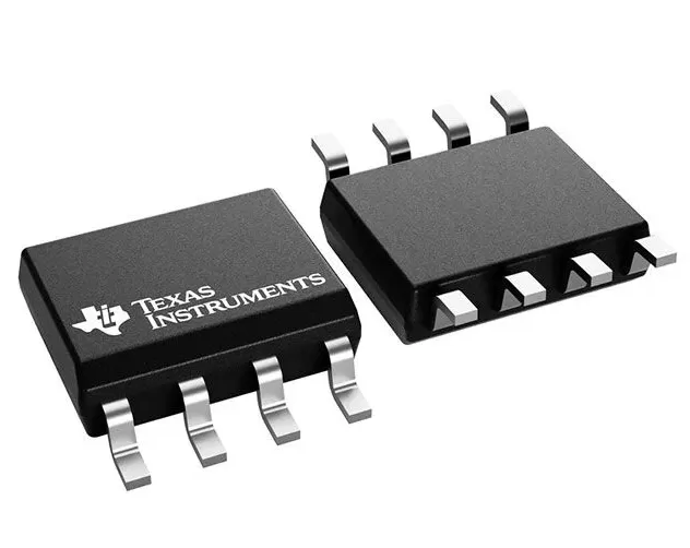

INA146UA2K5
Brand: Texas Instruments
Texas Instruments INA146UA2K5 is a power management component designed for Industrial Automation and related applications. In stock at Superb Automation — request a quote for competitive pricing and fast delivery.
Product Specifications
INA146UA2K5
Texas Instruments — Power Management & Signal Chain
Product Overview
The INA146UA2K5 from Texas Instruments is a power management / signal chain IC delivering high efficiency, precision regulation, and robust protection. Texas Instruments (TI) is a global leader in analog ICs, power management solutions, and embedded processors.
Superb Automation partners with leading brands including Qorvo, TI, ADI, XILINX, NVIDIA, Intel, ST, MACOM, Renesas, and Coilcraft to provide complete BOM and supply-chain solutions.
Key Features
- High-efficiency power conversion with low quiescent current
- Wide input voltage range with precision output regulation
- Integrated over-current, over-temperature, and short-circuit protection
- Small footprint packaging for space-constrained designs
- AEC-Q100 qualified options available for automotive applications
- Flexible sequencing and soft-start control
Key Specifications
| Input Voltage | V |
| Output Voltage | V |
| Output Current | A |
| Switching Frequency | kHz |
| Efficiency | % |
| Quiescent Current | µA |
| Topology | — |
| Package | — |
| Operating Temp | °C |
| Protection | — |
Applications
Industrial Automation
Automotive Electronics
Telecom Infrastructure
Server & Data Center Power
Medical Devices
Consumer Electronics
Request Quote — In Stock, 100% New & Original, Full Warranty
INA146UA2K5: the high voltage difference amplifier on a reel
INA146UA2K5 is INA146UA on a 2500 piece reel. The electrical rows are unchanged: plus or minus 100 volts of common mode at plus or minus 15 V, a gain of 0.1 from the on-die divider, 0.025 per cent gain error, 80 dB of rejection typical, and a bandwidth of 550 kHz at a gain of 0.1 falling to 50 kHz at unity gain.
The reel is where battery test equipment is bought, because those racks are built in tens and hundreds of channels and every channel needs the same attenuator. A part whose ratio is trimmed on the die at 0.025 per cent does not need a per channel gain calibration, and that is the economic case for buying the reel rather than building a divider.
INA146UA2K5 as the vendor document publishes it
| Gain | 0.1 V/V from the on-die divider, 0.1 to 100 with external resistors |
| Gain error | 0.025 per cent typical, 0.1 maximum |
| Gain drift | 1 ppm per degree typical, 10 maximum |
| Nonlinearity | 0.001 per cent typical, 0.01 maximum of full scale range |
| Offset at plus or minus 15 volts | 1 millivolt typical, 5 maximum |
| Offset at 5 volts | 3 millivolts typical, 10 maximum |
| Offset drift | 10 microvolts per degree maximum |
| Supply rejection | 100 microvolts per volt typical, 600 maximum |
| Common mode range at plus or minus 15 volts | minus 100 to plus 100 volts |
| Common mode range at 5 volts | minus 25 to plus 19 volts |
| Common mode rejection | 70 dB minimum, 80 typical, 64 over temperature |
| Input impedance | 110 kohm non-inverting, 91.7 kohm inverting, 55 kohm common mode |
| Bias current | 50 nanoamps maximum |
| Voltage noise | 12 microvolts peak to peak, 550 nanovolts per root hertz at 1 kHz |
| Bandwidth at a gain of 0.1 | 550 kHz, 50 kHz at unity gain |
| Slew rate | 0.45 volts per microsecond on SHE, 0.3 on TID |
| Settling to 0.01 per cent | 80 microseconds on a 10 V step |
| Quiescent current | 570 microamps typical on SHE, 250 on TID, 700 maximum |
| Supply range | 4.5 to 36 volts single, plus or minus 2.25 to plus or minus 18 dual |
| Body | eight pin SOIC |
| Temperature range | minus 40 to plus 85 degrees |
| Catalogue code | INA146UA2K5 |
| Carrier | 2500 piece reel, 2K5 suffix |
| Grade | UA, the only grade published for this family |
A gain of 0.1 to 100 from an external pair
The on-die network of INA146UA2K5 is a 10 to 1 divider, so with the output amplifier used as a unity gain buffer the differential gain is 0.1 V/V and the input can take plus or minus 100 volts. Gains above 0.1 are set with an external resistor pair, and the vendor is explicit that the external pair does not affect the common mode input range, because the divider that sets the range sits ahead of the gain stage.
That separation is the useful property. A user can take a plus or minus 100 volt differential, attenuate it to plus or minus 10 volts, and then add gain in the same stage without giving up the input window. The gain accuracy at 0.1 is 0.025 per cent typical and 0.1 maximum, with nonlinearity at 0.001 per cent typical and 0.01 maximum of full scale range, so the attenuator itself is better than most converters behind it.
550 kHz at 0.1 and 50 kHz at unity
The small signal bandwidth of INA146UA2K5 is 550 kHz at a gain of 0.1 and 50 kHz at a gain of 1, with a slew rate of 0.45 or 0.3 volts per microsecond depending on origin, a settling time of 40 microseconds to 0.1 per cent and 80 to 0.01 on a 10 V step, and a load capacitance limit of 1 nanofarad. Noise is 12 microvolts peak to peak from 0.1 to 10 Hz and 550 nanovolts per root hertz at 1 kHz, referred to the input.
Because the input is attenuated by ten, the output noise at a gain of 0.1 is a tenth of those figures, 55 nanovolts per root hertz, which is quiet enough for a 16 bit converter on a 10 V span. At a gain of 1 the same part delivers the full 550 nanovolts and the bandwidth falls by a factor of ten, which is the trade the external resistor pair makes: gain buys resolution and costs speed in the same proportion.
Two chip origins, 570 and 250 microamps
The electrical table of INA146UA2K5 is split by chip site origin. On the SHE origin the quiescent current is 570 microamps typical and 700 maximum, the slew rate 0.45 volts per microsecond, overload recovery 40 microseconds and short circuit current 15 milliamps. On the TID origin the same rows read 250 microamps, 0.3 volts per microsecond, 2 microseconds and 27 milliamps.
Those are not small differences in a battery instrument: 250 microamps against 570 is more than half the budget, and 2 microseconds of overload recovery against 40 changes the scan rate of a multiplexed channel. The offset and gain rows do not differ by origin, so a purchase decision that is made on accuracy alone will not see the split. INA146UA2K5 on an order pins the body and the grade, and the origin is only visible in the marking or on the reel label.
Plus or minus 100 volts of common mode at plus or minus 15 volts
INA146UA2K5 is built for the case where the common mode is far outside the supply. On plus or minus 15 volts the input common mode range is minus 100 to plus 100 volts; on a 5 V single supply it is minus 25 to plus 19 volts. The vendor describes that headroom as inherent input protection, and it is the reason the part appears in battery cell formation equipment and in AC drive control modules, where the measurement point sits at a rail that the signal chain does not share.
The range is not a constant: it moves with the reference and with the output. The vendor writes the window as 11 times the negative supply minus 10 times the reference, to 11 times the positive supply minus 1, minus 10 times the reference. That formula is the one to use when the reference is not at mid supply, because a reference offset of 2 V moves both ends by 20 V and a channel that was inside the window can leave it without anything else changing.
1 millivolt of offset at plus or minus 15 volts, 3 at 5 volts
Offset on INA146UA2K5 is 1 millivolt typical and 5 millivolts maximum on a plus or minus 15 volt supply, and 3 millivolts typical with 10 maximum on a 5 V supply. Drift is 10 microvolts per degree maximum over minus 40 to plus 85 degrees, supply rejection is 100 microvolts per volt typical and 600 maximum, and the offset of the output stage alone is 1 millivolt referred to the input.
At a gain of 0.1 those input errors are attenuated tenfold at the output, which is 100 to 500 microvolts, and the error that then dominates is the 0.025 per cent gain error across a 100 V input, 25 millivolts. That is the arithmetic that surprises people: on a high voltage attenuator the offset is not the problem, the gain error and the resistor ratio are, and a trim at one point on the range does not fix a ratio error at another.
80 dB of rejection behind a 10 to 1 divider
Common mode rejection on INA146UA2K5 is 70 dB minimum and 80 typical at 25 degrees, falling to 64 minimum and 74 typical over minus 40 to plus 85 degrees, measured from the negative window to the positive window with a zero ohm source. Eighty dB is a factor of ten thousand, so 100 volts of common mode becomes 10 millivolts of input referred error, which at a gain of 0.1 is 1 millivolt at the output.
That number is only reached with a balanced source. The divider is trimmed as a ratio, but any series resistance added to one input, from a protection resistor, a filter or a connector, unbalances the two paths and converts common mode into differential. The vendor's own circuit advice is that the source impedance at the two input terminals must be nearly equal, and on a high voltage input where the protection resistor is hundreds of ohms that advice is the difference between 80 dB and 60 dB.
Twenty five hundred pieces covers a rack build with spares, and the part is not a commodity that gets cheaper in volume, so the reel is a planning decision rather than a price one. Our safety stock planning page covers the quantity, and the date code management page covers ageing the stock between builds.
Does the reel version carry the same 100 volt window? Yes. The window is a property of the divider and the process, not of the carrier, and the reel does not change which chip origin is inside.
What is the highest common mode the part survives? The vendor specifies the input range to plus or minus 100 volts on plus or minus 15 V supplies, and describes that headroom as inherent protection. It is a range, not a transient rating, and a surge above it needs an external clamp.