


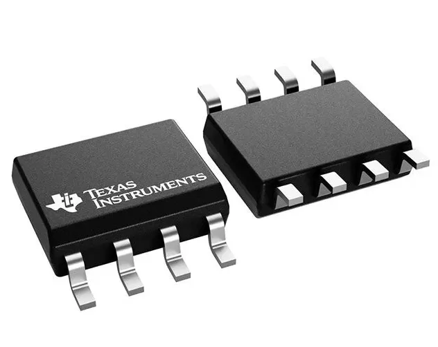

INA141UA2K5
Brand: Texas Instruments
Texas Instruments INA141UA2K5 is a power management component designed for Industrial Automation and related applications. In stock at Superb Automation — request a quote for competitive pricing and fast delivery.
Product Specifications
INA141UA2K5
Texas Instruments — Power Management & Signal Chain
Product Overview
The INA141UA2K5 from Texas Instruments is a power management / signal chain IC delivering high efficiency, precision regulation, and robust protection. Texas Instruments (TI) is a global leader in analog ICs, power management solutions, and embedded processors.
Superb Automation partners with leading brands including Qorvo, TI, ADI, XILINX, NVIDIA, Intel, ST, MACOM, Renesas, and Coilcraft to provide complete BOM and supply-chain solutions.
Key Features
- High-efficiency power conversion with low quiescent current
- Wide input voltage range with precision output regulation
- Integrated over-current, over-temperature, and short-circuit protection
- Small footprint packaging for space-constrained designs
- AEC-Q100 qualified options available for automotive applications
- Flexible sequencing and soft-start control
Key Specifications
| Input Voltage | V |
| Output Voltage | V |
| Output Current | A |
| Switching Frequency | kHz |
| Efficiency | % |
| Quiescent Current | µA |
| Topology | — |
| Package | — |
| Operating Temp | °C |
| Protection | — |
Applications
Industrial Automation
Automotive Electronics
Telecom Infrastructure
Server & Data Center Power
Medical Devices
Consumer Electronics
Request Quote — In Stock, 100% New & Original, Full Warranty
INA141UA2K5: the UA grade on a reel, and what the wider bin costs
INA141UA2K5 is the UA grade on a 2500 piece reel. Production volume usually lands here: the UA bin is the one stocked in depth, the reel is the carrier the line can run, and the electrical difference from the U grade is a wider offset window rather than a different function.
That difference is worth pricing rather than assuming. Two hundred and fifty microvolts at a gain of 10 is 2.5 millivolts at the output, and on a 4 V span it is 0.06 per cent, which a single point trim removes. The drift of 2.5 microvolts per degree does not trim out, and over a 45 degree swing it is 112 microvolts at the input, or 1.1 millivolts at the output, which is the number to carry in the error budget.
INA141UA2K5 as the vendor document publishes it
| Gain | 10 V/V with pin 1 open, 100 V/V with pin 1 shorted |
| Gain error, G = 10 | 0.15 per cent maximum |
| Gain error, G = 100 | 0.15 per cent maximum |
| Gain drift | 2 ppm per degree typical, 10 maximum |
| Offset, G = 10 | 250 microvolts maximum |
| Offset, G = 100 | 125 microvolts maximum |
| Offset drift | 2.5 microvolts per degree maximum |
| Common mode rejection, G = 100 | 110 dB minimum, 120 typical |
| Input bias current | 2 nanoamps typical, 5 maximum |
| Input impedance | 100 Gohm in parallel with 2 pF, differential |
| Bandwidth, G = 10 | 994 kHz on SHE, 610 kHz on TID |
| Bandwidth, G = 100 | 200 kHz |
| Slew rate, G = 10 | 4 volts per microsecond on SHE, 2 on TID |
| Settling to 0.01 per cent | 7 microseconds at G = 10, 9 at G = 100 |
| Overload recovery | 4 microseconds from a 50 per cent overdrive |
| Output swing | within 1.4 volts of each rail on SHE, 0.15 on TID |
| Quiescent current | 750 microamps typical, 800 maximum on SHE; 590 typical on TID |
| Supply range | plus or minus 2.25 to plus or minus 18 volts, 4.5 to 36 volts single |
| Stable load capacitance | 1000 picofarads |
| Short circuit current | 20 milliamps |
| Body | eight pin SOIC, D package |
| Temperature range | minus 40 to plus 85 degrees |
| Catalogue code | INA141UA2K5 |
| Carrier | 2500 piece reel, 2K5 suffix |
| Grade | UA, 250 microvolts at a gain of 10 |
SHE and TID: one part number, two different chips
The electrical table for INA141UA2K5 is split by chip site origin, SHE and TID, and the two columns are not interchangeable. At a gain of 10 the SHE reading is 100 microvolts maximum offset against 80 microvolts on TID, and the bandwidth is 994 kHz against 610 kHz. At a gain of 100 the SHE part settles in 9 microseconds against 7, and the quiescent current is 750 microamps against 590.
What the split really changes is the output stage. The SHE chip swings to within 1.4 V of each rail, the TID chip to within 0.15 V, so a channel that has to reach 4.5 V on a 5 V rail works on one origin and clips on the other. Because the body marking is the only visible difference, INA141UA2K5 on a purchase order pins the body but not the origin. A build that needs the wider output swing should say so on the order or screen the incoming lot; a build that only needs the offset does not care.
The reference pin has to see 8 ohms or better
The output of INA141UA2K5 is referred to the Ref pin, and the vendor is unusually specific about what that pin tolerates: 8 ohms in series with Ref drops common mode rejection to about 80 dB at a gain of 10. That is the pin a divider, a buffer or a ground return lands on, and a 1 kohm divider feeding it directly is three orders of magnitude outside the window. The reference has to come from an amplifier or from a solid ground, never from a resistor network.
The same rule applies to the strap in the previous section and to the input returns. On a single supply the reference sits at mid rail and the rejection figure now depends on that node holding still while the common mode moves, so the buffer that sets mid rail is part of the amplifier, not part of the power supply. On a dual supply the pin is grounded at the star point, and a separate analog ground that carries the reference current back is worth more than any capacitor on the pin.
A gain of 10 or 100 from a strap on pin 1
INA141UA2K5 has no gain resistor and no gain equation. The three op amp network and its resistors are trimmed on the die to a gain of 10 V/V, and a single pin decides whether the second stage is in or out: with the pin left open the gain is 10, with the pin shorted to the common point the gain is 100. Nothing else about the circuit changes, which is why the same board can serve a bridge channel at 10 and a thermocouple channel at 100 without a resistor change.
Two numbers decide whether that strap is a convenience or a trap. The vendor states that 0.5 ohm of series resistance in the strap reduces the gain by 0.1 per cent, so a mechanical jumper with a tired contact is already a gain error, and the strap should be a solder link or a zero ohm part rather than a header. The vendor also states that the internal resistors carry about 25 per cent of value spread, so gains between 10 and 100 set with an external resistor are uncertain and are not the intended use of INA141UA2K5.
7 microseconds to settle and 4 to recover
Settling on INA141UA2K5 is 7 microseconds to 0.01 per cent at a gain of 10 and 9 microseconds at a gain of 100, measured on a 5 V step. Overload recovery from a 50 per cent overdrive is 4 microseconds. The bandwidth is 994 kHz on the SHE chip and 610 on TID at a gain of 10, falling to 200 kHz at a gain of 100 on both.
For a multiplexed front end the sum of those numbers is the scan budget. Sixteen channels at 9 microseconds of settling plus the acquisition window of the converter is a few hundred microseconds per scan, which suits pressure, temperature and strain logging and does not suit a vibration channel above a few kilohertz. The recovery figure matters more than the settling figure in that calculation, because a multiplexer that switches from an open channel to a live one presents exactly the overdrive the recovery row describes.
100 microvolts at a gain of 10, 50 at a gain of 100
Offset on INA141UA2K5 is quoted per gain and per grade, and the pairs are the whole selection story. At a gain of 10 the U grade is 100 microvolts maximum and the UA grade 250; at a gain of 100 the same two grades read 50 and 125 microvolts. Drift runs 2 microvolts per degree maximum on the U grade and 2.5 on the UA, and the drift window is specified over minus 40 to plus 85 degrees.
The counterintuitive part is that the offset improves as the gain rises, because the input stage dominates the error and its contribution is referred back through the first stage. A 250 microvolt UA part at a gain of 10 is 2.5 millivolts at the output, which on a 4 V span is 0.06 per cent and can be trimmed once. Its 2.5 microvolts per degree is 100 microvolts over a 40 degree swing at the input, 1 millivolt at the output, which cannot be trimmed once and has to be budgeted.
800 microamps, plus or minus 2.25 to 18 volts and the D body
INA141UA2K5 draws 800 microamps maximum, 750 typical on the SHE chip and 590 on TID, from a supply anywhere between plus or minus 2.25 and plus or minus 18 volts, or 4.5 to 36 volts single. That window is wide enough to run from an unregulated 24 V rail with margin and narrow enough at the bottom to run from a 5 V rail with the reference at mid supply. The part is stable into 1000 picofarads and limits short circuit current at 20 milliamps.
The body is the eight pin SOIC, the D package, which on INA141UA2K5 is the only body offered in this catalogue entry. Thermal resistance is 150 degrees per watt in still air, so 800 microamps at 30 volts total, 24 milliwatts, raises the junction 4 degrees, and the package is not the limit at any supply in the window. What the small body does limit is the copper available to the reference pin, which is why that pin wants a short trace to the buffer rather than a long one to the ground plane.
The reel is the carrier that keeps a line running, and it is also the carrier that has to be dry packed and tracked once it is opened. Level 3 with a 168 hour floor life is the row to look for on the label, and the label is the only record of it. Our incoming inspection plan covers what a lot record should capture on arrival, and the traceability report page covers what has to travel with the reel through the build.
Why does the part get cheaper as the offset gets worse? Because the UA bin is what is left after the tighter parts are sorted out, and the sort is the cost. The silicon is the same and the function is the same; only the tested window differs, and that window is what a calibration has to cover.
Can a UA part be used where the bill of materials says U? Only with a deviation, because the offset and the rejection limits are different rows and an inspector comparing labels will see the difference. Our drop in replacement check page sets out the rows to compare before that deviation is written.