


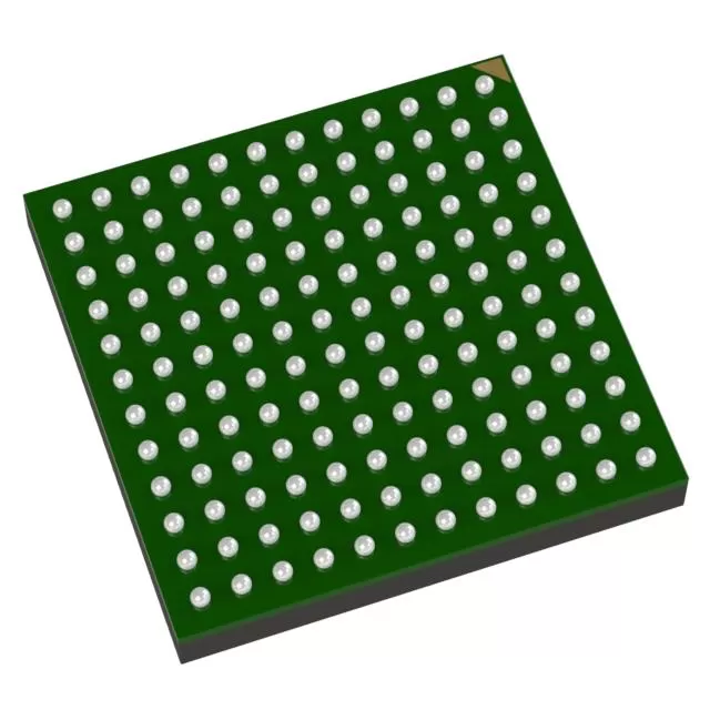

MAX9867ETJ+T
Brand: Analog Devices
Analog Devices MAX9867ETJ+T is a analog & mixed-signal component designed for Precision Instrumentation and related applications. In stock at Superb Automation — request a quote for competitive pricing and fast delivery.
Product Specifications
MAX9867ETJ+T
Analog Devices — Analog & Mixed-Signal ICs
Product Overview
The MAX9867ETJ+T from Analog Devices is a high-performance analog / mixed-signal IC providing precision signal acquisition, conversion, and conditioning. Analog Devices (ADI) is a world leader in high-performance analog, mixed-signal, and DSP ICs for instrumentation, healthcare, automotive, and communications.
Superb Automation partners with leading brands including Qorvo, TI, ADI, XILINX, NVIDIA, Intel, ST, MACOM, Renesas, and Coilcraft to provide complete BOM and supply-chain solutions.
Key Features
- High-resolution data conversion with excellent SNR and THD
- Wide dynamic range and high linearity across operating conditions
- Integrated voltage reference with low temperature drift
- Flexible digital interface — SPI, I2C, or parallel options
- Industrial/automotive temperature range with guaranteed specs
- Low power consumption with power-down modes
Key Specifications
| Resolution | bits |
| Channels | — |
| Sample Rate | kSPS |
| Interface | — |
| Supply Voltage | V |
| Operating Temp | °C |
| Package | — |
| INL | LSB |
| SNR | dB |
| THD | dB |
Applications
Precision Instrumentation
Industrial Process Control
Medical Imaging & Diagnostics
Automotive Sensor Interfaces
Communications Infrastructure
Test & Measurement
MAX9867ETJ+T: a 1.8 V codec that draws 3.7 mA until headphones are plugged in
The MAX9867ETJ+T is an Analog Devices stereo audio codec built for portable products, running from a single 1.8 V supply with a digital interface supply anywhere from 1.65 V to 3.6 V. Playback consumption is 6.7 mW, the stereo DAC is specified at 90 dB and the stereo ADC at 85 dB across 8 kHz to 48 kHz sampling. The part carries stereo differential microphone inputs that accept analog or digital microphones, single-ended line inputs with a configurable preamplifier, an auxiliary ADC that can track any DC voltage such as a battery cell, and stereo headphone amplifiers that work in differential, single-ended or capacitorless mode. The capacitorless configuration delivers 10 mW into 32 ohm without a coupling capacitor. It is packaged in a 30-bump wafer level package measuring 2.2 mm by 2.7 mm on a 0.4 mm pitch. It sits with the converters it pairs with on the analog and mixed-signal IC line card.
The quiescent current and the load current are on different scales
At 1.8 V, 6.7 mW is 3.72 mA for the whole codec in playback. Driving 10 mW into 32 ohm takes 0.566 V rms and 17.7 mA rms, which is 25 mA at the peak of the waveform. So a product with headphones connected draws several times what the datasheet playback figure suggests, and the headphone load, not the codec, sets the battery curve. The capacitorless output removes two coupling capacitors and their leakage, and it also removes the DC bias that those capacitors were blocking, so the amplifier sits at midrail on the load.
| Parameter | Vendor figure | Derived figure |
|---|---|---|
| Playback power | 6.7 mW | 3.72 mA at 1.8 V |
| Headphone output | 10 mW into 32 ohm, capacitorless | 0.566 V rms, 17.7 mA rms, 25 mA peak |
| DAC performance | 90 dB stereo | 14.7 bits of usable range |
| ADC performance | 85 dB stereo | 13.8 bits of usable range |
| Sample rates | 8 kHz to 48 kHz | voiceband filter, stopband over 70 dB |
| Master clock | 10 MHz to 60 MHz | 16.7 ns period at the top of the range |
| Body | 2.2 mm by 2.7 mm, 30 bumps | 0.4 mm pitch, 5.9 sq mm of board |
A 0.4 mm pitch package is an assembly constraint, not a footnote
A 30-bump wafer level package on 0.4 mm pitch needs a stencil and a placement machine rated for that pitch, and it needs the pad geometry from the vendor land pattern rather than a scaled version of it. For a product built in the hundreds this is routine; for a prototype line running 0.5 mm pitch parts it is a process change. The 2.2 mm by 2.7 mm body is 5.9 sq mm, which is why the part is chosen in the first place, and the same body has no room for a large decoupling capacitor underneath, so the 1.8 V bypass has to sit beside it.
Clock, interface and the auxiliary converter
- Any master clock from 10 MHz to 60 MHz is accepted, so the codec can be clocked from the application processor without a dedicated crystal.
- The audio bus is I2S or TDM compatible, which allows several codecs or a codec and a modem voice path on the same lines.
- The auxiliary ADC is a separate measurement path, useful for a battery or a thermal node, and it does not interrupt audio.
- Click and pop suppression covers volume changes and power-up, which is the specification a listener notices before any distortion number.
Questions buyers ask
Does capacitorless mode need a different headphone jack? It needs a jack whose sleeve can sit at midrail rather than at ground, and the accessory detection has to tolerate that. The gain in board area is two capacitors per channel.
Is the 90 dB figure the dynamic range or the signal to noise ratio? The vendor states it as DAC performance, so treat it as the usable converter range and read the test conditions in the datasheet before placing it in a budget.
Portable audio builds usually buy the codec with its passives and connector as one kit, and the cost side of that bundle is covered on how to reduce component cost and on the amplifier cross reference page for the headphone stage.
MAX9867ETJ+T: a separate 1.65 V to 3.6 V interface rail, and a master clock from 10 to 60 MHz
The digital interface supply is specified from 1.65 V to 3.6 V while the analog side runs from a 1.8 V single supply, and the master clock can be anything between 10 MHz and 60 MHz. Those two sentences decide the board: the codec can sit on a 3.3 V logic bus and still be powered from the same 1.8 V rail as the rest of the audio block, and the clock does not have to be a 12.288 MHz crystal because the part accepts a range and generates the audio clocks from it. A system that has a 26 MHz reference from a cellular modem can use it directly.
| Item | Published value | Arithmetic or consequence |
|---|---|---|
| Supply | 1.8 V single supply | 3.7 mA at 1.8 V for the 6.7 mW playback figure |
| Interface rail | 1.65 V to 3.6 V separate | No level shifter between a 3.3 V host and the codec |
| Master clock | 10 MHz to 60 MHz | 26 MHz or 24 MHz system clocks are inside the range |
| Sample rate | 8 kHz to 48 kHz | 48 kHz at 256 times the rate needs 12.288 MHz derived inside |
| Converters | 90 dB DAC, 85 dB ADC | About 14.6 and 13.8 effective bits on a full scale signal |
| Headphone | Differential, single ended or capacitorless | The capacitorless mode removes two large parts from the board |
| Body | 30-bump 2.2 by 2.7 mm, 0.4 mm pitch | 0.4 mm pitch needs a stencil and reflow profile that match |
Deriving the audio clock from an unrelated reference has a jitter cost
Accepting a 10 to 60 MHz master clock is convenient, and the jitter of that clock becomes part of the converter's noise floor. A 26 MHz reference shared with a radio has phase noise that is fine for a voice channel and marginal for a 90 dB converter, so the choice is between a dedicated crystal and an accepted noise floor. That trade is the reason the specification lists the clock range rather than a single frequency.
Capacitorless headphone drive moves the cost to the package
Removing the output coupling capacitors saves board area and removes a low frequency corner, and it puts a charge pump inside the part, which is where the 0.4 mm pitch package comes from. The consequence for assembly is that the 30-bump WLP needs a stencil aperture and a reflow profile that are qualified for the pitch, and a line that has only run 0.5 mm pitch parts has a process change to make before the first build.
Buying this order code
The TJ suffix is the wafer level package and the plus sign marks the reel, so the code carries both. The audio and codec family sits on the analog line card, pin compatible codec options are compared on the pin to pin page, and the reel and date code are confirmed through the lead time desk.
Request Quote — In Stock, 100% New & Original, Full Warranty