


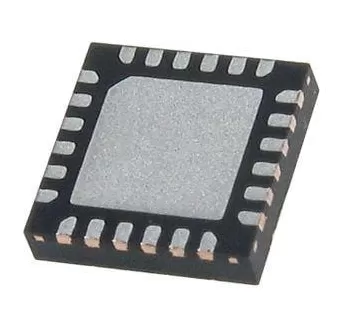

TPSM84209RKHR
Brand: Texas Instruments
Texas Instruments TPSM84209RKHR is a power management component designed for AI Servers & Low-Altitude Economy (Drone and UAV) and related applications. In stock at Superb Automation — request a quote for competitive pricing and fast delivery.
Product Specifications
TPSM84209RKHR
Texas Instruments — Power Management & Signal Chain
Product Overview
The TPSM84209RKHR from Texas Instruments is a power management / signal chain IC delivering high efficiency, precision regulation, and robust protection. Texas Instruments (TI) is a global leader in analog ICs, power management solutions, and embedded processors.
Superb Automation partners with leading brands including Qorvo, TI, ADI, XILINX, NVIDIA, Intel, ST, MACOM, Renesas, and Coilcraft to provide complete BOM and supply-chain solutions.
Key Features
- High-efficiency power conversion with low quiescent current
- Wide input voltage range with precision output regulation
- Integrated over-current, over-temperature, and short-circuit protection
- Small footprint packaging for space-constrained designs
- AEC-Q100 qualified options available for automotive applications
- Flexible sequencing and soft-start control
Key Specifications
| Input Voltage | V |
| Output Voltage | V |
| Output Current | A |
| Switching Frequency | kHz |
| Efficiency | % |
| Quiescent Current | µA |
| Topology | — |
| Package | — |
| Operating Temp | °C |
| Protection | — |
Applications
Industrial Automation
Automotive Electronics
Telecom Infrastructure
Server & Data Center Power
Medical Devices
Consumer Electronics
Request Quote — In Stock, 100% New & Original, Full Warranty
TPSM84209RKHR: 2.5 A step-down power module with the inductor inside a 4.5 by 4 mm QFN
TPSM84209RKHR is a complete step-down converter in the nine pin RKH body that accepts 4.5 V to 28 V, delivers 2.5 A, switches at 750 kHz nominal and includes the inductor and the passives inside a 4.5 mm by 4 mm by 2 mm package in a QFN body of 9 pins. The TPSM84209 is a power module rather than a controller: the inductor and the passive components are inside a 4.5 mm by 4 mm by 2 mm QFN, so the board carries an input capacitor, an output capacitor and the feedback divider. Input is 4.5 V to 28 V with a 3.8 V under voltage lockout, output is set by two resistors, and the rated current is 2.5 A at a 750 kHz switching frequency. The minimum input is 4.5 V or 1.3 times the output, whichever is greater, which is the rule that keeps the high side switch able to turn on.
Order code and package
| Order code | TPSM84209RKHR |
| Function | step-down power module with integrated inductor |
| Input voltage | 4.5 V to 28 V, minimum also 1.3 times the output |
| Output current | 2.5 A |
| Output voltage | set by an external divider |
| Switching frequency | 578 kHz to 923 kHz, 750 kHz typical |
| Input under voltage lockout | 3.8 V rising |
| Package | nine pin QFN, 4.5 mm by 4 mm by 2 mm |
| Soft start | internal |
| Ambient temperature range | minus 40 C to 85 C |
Electrical parameters that decide the application
| Thermal resistance, junction to ambient | 32.7 C per W on a 63 mm by 50 mm four layer board with 2 oz copper |
| Junction to top characterization parameter | 2.2 C per W |
| Junction to board characterization parameter | 17 C per W |
| Input capacitor in the reference circuit | 10 uF, 50 V, 1210 ceramic plus 100 uF, 35 V electrolytic |
| Output capacitor in the reference circuit | two 47 uF, 16 V, 1210 ceramic |
| Enable pull-up current | 0.7 uA at 1 V |
| Enable hysteresis current | 1.55 uA at 1.5 V |
| Reference conditions | 12 V in, 3.3 V out, 2.5 A, 25 C ambient |
Points to check before this part goes on a BOM
A module moves the switching loop, the inductor and the compensation inside the package, and what it asks in return is that the board does not spoil them. The input capacitor has to be close to the input pins because the loop area between the capacitor and the internal switches is what radiates; the output capacitor sets the transient response; and the feedback divider is the only part of the control that remains outside, so its tolerance is the output tolerance.
The 32.7 C per W junction to ambient figure is measured on a 63 mm by 50 mm four layer board with 2 oz copper in natural convection, which is a generous board. On a small card with two layers the number is worse and the 2.5 A rating becomes a thermal question. At 2.5 A from 12 V to 3.3 V the loss is roughly a watt, so the rise on the reference board is about 33 C and the same loss on a poor board is double that.
The minimum input rule of 4.5 V or 1.3 times the output is the constraint that a 5 V output from a 5 V bus violates. A 5 V rail cannot produce 5 V through a buck stage, and 1.3 times 5 V is 6.5 V, so a 5 V output needs at least 6.5 V in. That rule is not a quirk of this module; it is the headroom the high side switch needs to turn on, and a board that ignores it produces a rail that drops out under load and looks like a current limit problem.
The switching frequency window of 578 kHz to 923 kHz around a 750 kHz nominal is wide enough that a filter placed for the nominal is not centred on the actual. The spread is the price of an internal oscillator without a trim, and it means the input filter and any snubber should be chosen for the band rather than for a single frequency. It also means two modules on the same board beat against each other unless they are synchronised, which this part does not offer.
A module is a schedule decision as much as an electrical one. A discrete converter needs an inductor selection, a compensation calculation, a loop measurement and a board review, and each of those is engineering time. This part replaces that work with a datasheet circuit and a set of capacitor values, at the cost of a fixed switching frequency, a fixed current rating and a package that cannot be reworked with a different inductor when the load changes.
The nine pin QFN has the inductor inside, so the height is 2 mm and the footprint is 18 square millimetres. That is a real constraint on a low profile card and it is the reason some products stay with a discrete converter and a low profile inductor. Where height is available, the module wins on area and on the number of components that have to be sourced and inspected.
The enable pin has a 0.7 uA pull-up and a 1.55 uA hysteresis current, which means a divider can set a precise turn on point and the pin does not float. On a 24 V bus that matters: the module should not start until the bus is above the point where the output can be regulated, and with a 3.8 V lockout and a 1.3 times output rule the divider is normally set well above both so that the module starts once and stays on rather than hunting at the threshold.
Where this order code fits
This order code belongs on industrial and telecom boards where the power stage has to fit in a small area and the engineering time for a discrete converter is not available: sensor interfaces, fieldbus nodes, small motor drives, test instruments and add-on cards. It is chosen when the input is a 12 V or 24 V bus, the output is 5 V or 3.3 V at a couple of amps, and the board risk of a discrete switcher is the thing being avoided. Teams comparing it with a neighbouring part start from our Power Management Cross Reference page, and teams replacing a part that has gone end of life start from the One Stop BOM Sourcing page.
Questions buyers ask
Can this module make 5 V from a 5 V input? No. The minimum input is 4.5 V or 1.3 times the output, whichever is greater, so a 5 V output needs 6.5 V at the input. A 5 V bus is therefore not a source for a 5 V rail through this part; it needs a boost or a buck-boost. The same rule applies to a 3.3 V output from a 5 V bus, which needs 4.29 V and is satisfied with 700 mV of margin.
What sets the output voltage? Two external resistors in the feedback divider. Everything else is inside the module, so the output tolerance is the module tolerance plus the divider tolerance, and a 1 percent pair is the right choice. A divider that is noisy or has long traces injects noise into the feedback node, which is the one place where a module is as sensitive as a discrete converter.
How much board area does it need? The body is 18 square millimetres, and the capacitors around it need roughly the same again to be effective. The reference circuit uses a 10 uF ceramic plus a 100 uF electrolytic at the input and two 47 uF ceramics at the output, so the practical footprint including the passives is closer to 40 square millimetres on a four layer board.
Is 2.5 A available at 85 C ambient? The 2.5 A rating is stated at a 25 C ambient on the reference board. At 85 C the loss that the package can dissipate is much smaller, so the current has to be derated. The junction to ambient figure of 32.7 C per W gives the arithmetic: at 85 C ambient there are 40 C left to the 125 C junction, which is about 1.2 W, and 1.2 W at 12 V to 3.3 V is roughly 2 A.
SUPERB holds and sources this line for production and repair demand, quoted against the exact ordering string with date codes, packing and country of origin stated on the offer. When a part is moving, the Component Lead Time Solutions page sets out the checks that keep a substitute from failing on the bench.

