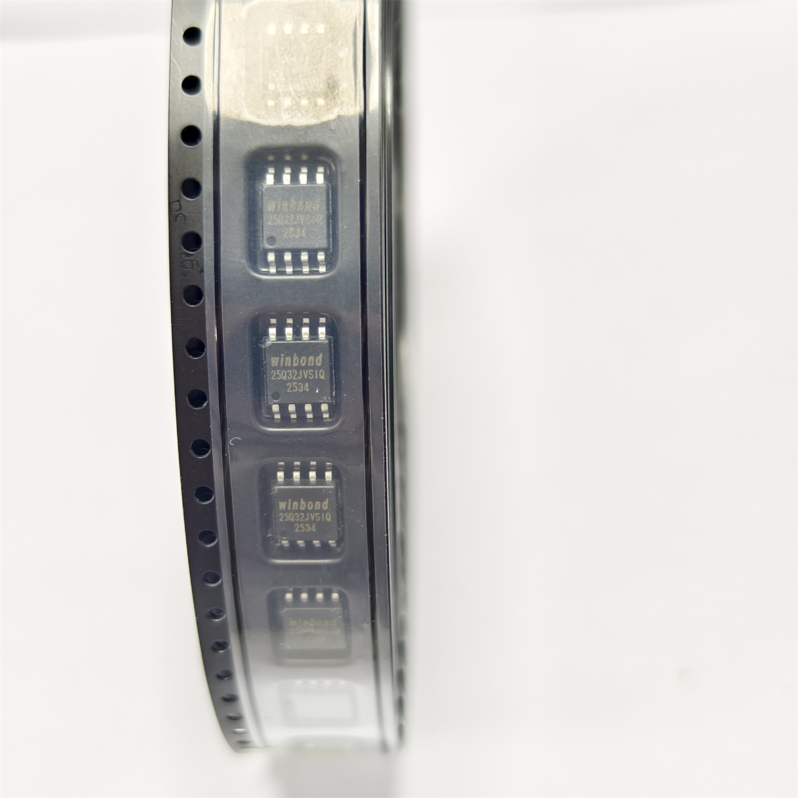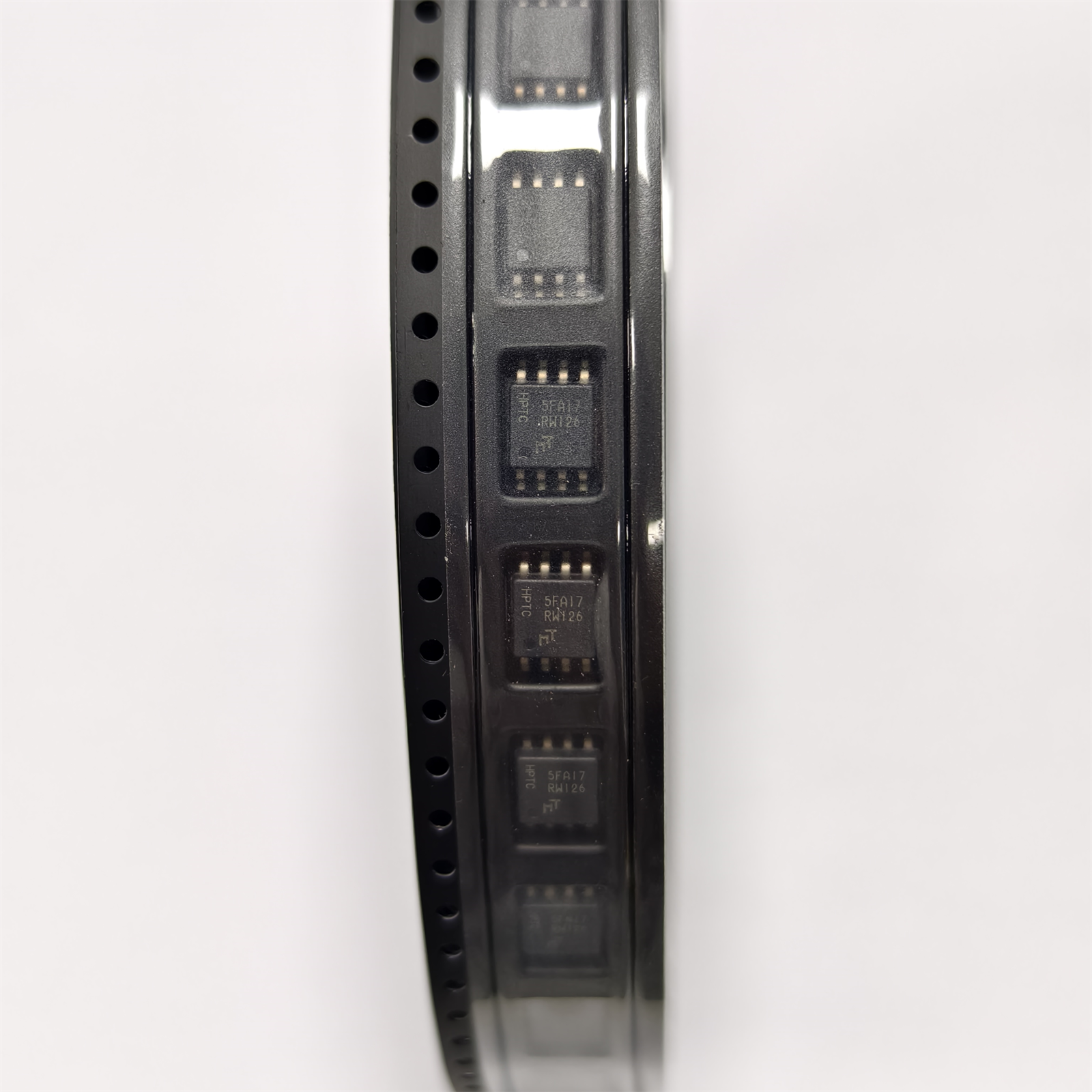

W25Q64JVSSIQ
The W25Q64JVSSIQ is Winbond's 64Mbit (8MB) serial NOR Flash memory from the JV series, delivering high-speed code and data storage for embedded systems. It supports standard SPI, Dual SPI, Quad SPI, QPI (Quad Peripheral Interface), and DTR (Double Transfer Rate) — achieving up to 532 Mbit/s effective throughput in Quad SPI mode at 133 MHz. Organized as 8M × 8 bits with uniform 4KB sectors, it provides fine-grained erase flexibility for applications mixing firmware storage with parameter data. The device is rated for 100,000 program/erase cycles minimum per sector with 20+ years data retention, operates from a single 2.7V–3.6V supply, and is specified over the full -40°C to +85°C industrial temperature range. Packaged in a standard 8-SOIC (208 mil) footprint, it is the most widely adopted NOR Flash chip in the embedded industry — the default external flash on ESP32 modules, the go-to code storage for STM32 and FPGA designs, and a staple in IoT, industrial control, and consumer electronics.
Product Specifications
W25Q64JVSSIQ — Winbond 64Mbit SPI NOR Flash Memory
Winbond Electronics — 64Mbit (8MB) Serial NOR Flash, SPI/Dual/Quad/QPI/DTR, 133MHz, 4KB Uniform Sectors, 100K P/E, 8-SOIC
MFR Part #: W25Q64JVSSIQ
Superb SKU: SB-W25Q64JVSSIQ
In Stock
The W25Q64JVSSIQ is Winbond's 64Mbit (8MB) serial NOR Flash memory from the JV series, delivering high-speed code and data storage for embedded systems. It supports standard SPI, Dual SPI, Quad SPI, QPI (Quad Peripheral Interface), and DTR (Double Transfer Rate) — achieving up to 532 Mbit/s effective throughput in Quad SPI mode at 133 MHz. Organized as 8M × 8 bits with uniform 4KB sectors, it provides fine-grained erase flexibility for applications mixing firmware storage with parameter data. The device is rated for 100,000 program/erase cycles minimum per sector with 20+ years data retention, operates from a single 2.7V–3.6V supply, and is specified over the full -40°C to +85°C industrial temperature range. Packaged in a standard 8-SOIC (208 mil) footprint, it is the most widely adopted NOR Flash chip in the embedded industry — the default external flash on ESP32 modules, the go-to code storage for STM32 and FPGA designs, and a staple in IoT, industrial control, and consumer electronics.
Key Performance Highlights
Memory Density
64 Mbit (8 MB)
Max Clock (Quad)
133 MHz (532 Mbps)
Endurance
100K P/E Cycles
Sector Size
4 KB Uniform
Supply Voltage
2.7 V – 3.6 V
Package
8-SOIC (208 mil)
Technical Specifications
Source: Winbond W25Q64JV datasheet (Revision J) & Mouser 454-W25Q64JVSSIQ
| Manufacturer | Winbond Electronics Corporation |
| MFR Part Number | W25Q64JVSSIQ |
| Memory Type | NOR Flash — Serial (SPI) |
| Product Series | W25Q64JV — spiFlash JV Series |
| Density | 64 Mbit = 8 MB |
| Organization | 8M × 8 bits |
| Interface Modes | Standard SPI / Dual SPI / Quad SPI / QPI / DTR (Double Transfer Rate) |
| Max Clock (SPI / Dual / Quad) | 133 MHz (532 Mbps effective in Quad mode) |
| Sector Size | 4 KB (uniform) — 2,048 sectors total |
| Block Size | 32 KB (½ block) / 64 KB (standard block) — 128 / 256 blocks |
| Page Size | 256 bytes — up to 256 bytes programmed per page command |
| Page Program Time (typ.) | 0.7 ms |
| Sector Erase Time (typ.) | 45 ms (4 KB), 120 ms (32 KB), 150 ms (64 KB) |
| Chip Erase Time (typ.) | 20 seconds |
| Endurance (min.) | 100,000 program/erase cycles per sector |
| Data Retention | 20 years (minimum) |
| Supply Voltage | 2.7 V to 3.6 V |
| Active Read Current | ~4 mA (typ., Quad SPI @ 133 MHz) |
| Standby Current | 1 µA (typ.) |
| Deep Power-Down Current | < 1 µA |
| Operating Temperature | -40°C to +85°C (Industrial) |
| Package / Case | 8-SOIC (208 mil / 5.28mm Wide) |
| Mounting Type | Surface Mount (SMD/SMT) |
| Packaging | Tube (standard) / Tape & Reel (W25Q64JVSSIQ TR) |
| Unique ID / Security | 64-bit unique serial number + 3× 256-byte OTP security registers |
| Mouser Part # | 454-W25Q64JVSSIQ |
Product Details
Product Description
The W25Q64JVSSIQ is Winbond's 64Mbit JV-series NOR Flash, representing the latest generation of the industry-standard W25Q family. It supports a full interface stack — standard SPI for legacy compatibility, Dual SPI and Quad SPI for higher throughput, and QPI (Quad Peripheral Interface) for reduced command overhead. The JV series adds DTR (Double Transfer Rate) mode, clocking data on both edges of SCK for twice the bandwidth at the same clock frequency.
The memory array is organized as 2,048 uniform 4KB sectors, enabling granular erase operations — ideal for designs that mix read-mostly firmware with frequently updated parameters. The 100,000 P/E cycle endurance (minimum) at 20+ years retention exceeds the requirements of most embedded products. The device operates from a single 2.7V–3.6V rail and drops to just 1µA in standby, making it suitable for battery-powered IoT endpoints. A 64-bit unique ID and three 256-byte OTP security registers provide device authentication and secure key storage.
Common Applications
MCU Firmware Storage — External code flash for STM32, ESP32, nRF52, and other MCUs with QSPI controllers
FPGA Configuration Memory — Bitstream storage for Xilinx, Intel/Altera, Lattice, and Gowin FPGAs
IoT OTA Firmware Updates — Dual-bank partition for A/B firmware swap with rollback support
Bootloader & Recovery — Second-stage bootloader storage for secure boot chains
Data Logging & Event Recording — Parameter storage, calibration tables, event logs in industrial equipment
Consumer Electronics — Set-top boxes, smart TVs, gaming accessories, audio DSP firmware
W25Q64JV Series — Package & Temperature Variants
The W25Q64JV family is available in multiple packages and temperature grades. The suffix decodes as follows:
| Ordering Code | Package | Temperature | Notes |
|---|---|---|---|
| W25Q64JVSSIQ | 8-SOIC 208 mil (Tube) | -40°C to +85°C | Most common variant — standard industrial |
| W25Q64JVSSIQ TR | 8-SOIC 208 mil (T&R) | -40°C to +85°C | Tape & Reel for automated assembly |
| W25Q64JVSSIM | 8-SOIC 208 mil | -40°C to +105°C | Extended temp — automotive/industrial |
| W25Q64JVXGIQ | XSON 6×5mm | -40°C to +85°C | Smaller footprint — space-constrained designs |
| W25Q64JVZPIQ | WSON 6×5mm | -40°C to +85°C | QFN-style exposed pad — better thermal |
W25Q64JVSSIQ vs Alternative 64Mbit NOR Flash
| Parameter | W25Q64JVSSIQ | W25Q64FWSSIQ | MX25L6433F | GD25Q64ESIG |
|---|---|---|---|---|
| Manufacturer | Winbond | Winbond | Macronix | GigaDevice |
| Family / Series | JV Series (DTR + QPI) | FW Series (Legacy) | MX25L Series | GD25Q Series |
| Max Clock (Quad) | 133 MHz | 104 MHz | 133 MHz | 120 MHz |
| DTR Mode | Yes | No | No (DTR on MX25L6436F) | No |
| QPI Support | Yes | Partial | Yes (QPI mode) | Yes (QPI mode) |
| Endurance (P/E) | 100K cycles | 100K cycles | 100K cycles | 100K cycles |
| Package | 8-SOIC 208 mil | 8-SOIC 208 mil | 8-SOIC 208 mil | 8-SOIC 208 mil |
| Positioning | Best features: DTR+QPI+133MHz | Legacy — use JV for new designs | Strong alternative — wide 1.8V options | Cost leader — 120MHz max |
Cross-Supplier Note: All four devices share the same 8-SOIC 208 mil footprint and pinout for basic SPI operation (CS#, SO/SIO1, WP#/SIO2, GND, SI/SIO0, SCK, HOLD#/SIO3, VCC). Verify Quad Enable bit position (Status Register bit 9 / S9) and DTR/QPI command codes when designing for multi-source procurement. Winbond JV-series QE bit may be factory-set; Macronix and GigaDevice typically require software QE enable.
Why Source W25Q64JVSSIQ from Superb Automation
100% New & Original — trusted Channels
Every W25Q64JVSSIQ ships from Winbond-trusted supply chains with full lot traceability and certificate of conformance.
Tube or T&R — Production-Ready Packaging
Standard tube for prototyping and low volume; W25Q64JVSSIQ TR tape & reel (2,000 pcs/reel) for automated SMT lines.
Global Logistics — Same-Day Dispatch
Shenzhen and Hong Kong warehouses. FedEx/DHL/UPS express worldwide. In-stock NOR Flash ships same day.
Pre-Programming & Flash Services
Need firmware pre-programmed onto W25Q64JVSSIQ before assembly? Superb can coordinate batch programming of SPI NOR Flash with your binary image.
Competitive Volume Pricing
Prototype to high-volume production: 10 pcs to 100k+ units. W25Q64JV is a commodity NOR Flash — Superb offers aggressive volume quotes.
PCB & PCBA Integration
Components + PCB fabrication (16–60L, HDI) + turnkey SMT assembly — one supplier for your entire embedded system BOM.
PCB Design Considerations for SPI NOR Flash
SPI Bus Layout: At 133 MHz, SPI clock edges are only 3.75 ns apart. Superb recommends controlled-impedance 50Ω traces for SCK, with matched-length SI/SO lines (±2mm max skew). Series termination resistors (22Ω–33Ω) placed near the MCU driver help suppress reflections on longer traces.
SOP-8 Pad Design: The 8-SOIC 208 mil package uses standard 1.27mm pin pitch. Superb's laser-cut stencils use standard apertures for SOP-8 with sufficient toe fillet allowance. For high-volume production, W25Q64JVSSIQ TR (tape & reel) is recommended for pick-and-place compatibility.
Power Decoupling: A 100nF + 10µF decoupling pair within 3mm of VCC pin (pin 8) is recommended. The 10µF capacitor handles the brief current surge during program/erase operations (~15–20 mA). Superb supports 0402 and 0603 placement for tight decoupling.
Multi-Flash Array Design: For systems requiring > 64Mbit, multiple W25Q64JVSSIQ can share a common SPI bus with individual CS# lines. Superb's 4–60 layer PCB capability supports dense multi-chip memory arrays with controlled fan-out for CS# routing.
Frequently Asked Questions
What is the W25Q64JVSSIQ used for?
The W25Q64JVSSIQ is a 64Mbit serial NOR Flash chip used for storing MCU firmware, FPGA configuration bitstreams, bootloader code, OTA update partitions, data logs, and calibration parameters in embedded systems. It communicates over SPI at up to 133 MHz and is the most common external flash for ESP32, STM32, and FPGA designs.
What does JV mean in W25Q64JVSSIQ?
JV designates the JV-series, Winbond's current-generation NOR Flash family. It adds DTR (Double Transfer Rate) mode and full QPI (Quad Peripheral Interface) support over the previous FW series. The JV series delivers higher throughput (532 Mbps effective vs 416 Mbps on FW) at the same 8-SOIC footprint. It is the recommended choice for all new embedded designs.
Can W25Q64JVSSIQ replace W25Q64FWSSIQ?
Yes, in most designs. Both are 64Mbit, 3V, 8-SOIC with identical pinout. Standard SPI and basic Quad SPI read commands are fully backward-compatible. Key differences: JV supports DTR and QPI (new commands), and the QE (Quad Enable) bit may be factory-set on JV. If your firmware only uses standard SPI/Dual/Quad read commands and explicitly configures the status register, the JV is a drop-in upgrade from FW.
How many erase cycles can the W25Q64JVSSIQ handle?
The W25Q64JVSSIQ is rated for a minimum of 100,000 program/erase cycles per sector with 20+ years data retention. For a 4KB sector erased once per day, this gives ~274 years before hitting the endurance limit. In practice, wear-leveling algorithms (e.g., LittleFS, SPIFFS) distribute writes across sectors, extending the effective lifetime of the entire flash array well beyond the per-sector specification.
What MCU platforms use the W25Q64JVSSIQ?
The W25Q64 is one of the most widely supported NOR Flash chips. It is the default external flash on many ESP32 and ESP8266 modules, supported by STM32Cube/SPI and STM32 QSPI HAL drivers, compatible with Linux MTD subsystem via spi-nor driver, used as FPGA configuration flash for Xilinx and Intel/Altera devices, and supported by Arduino SPIFFS/LittleFS libraries. Winbond's official driver is available on GitHub.
Winbond vs Macronix vs GigaDevice: which 64Mbit NOR Flash to choose?
Choose Winbond W25Q64JVSSIQ for the best combination of features (DTR+QPI+133MHz), widest MCU ecosystem support, and long-term availability. Choose Macronix MX25L6433F if you need 1.8V operation or second-source options with minimal requalification. Choose GigaDevice GD25Q64ESIG for the most cost-sensitive designs — it is typically the lowest-priced option but runs at 120MHz max and has a smaller software ecosystem. All three are 8-SOIC pin-compatible for basic SPI operation.
Related Products
Superb Automation maintains supply of Winbond NOR Flash across multiple capacities and complementary memory components:
W25Q64JVSSIQ TR
Same chip in tape & reel (2,000 pcs/reel) for SMT lines
W25Q128JVSIQ
128Mbit (16MB) JV-series, same 8-SOIC footprint, 2× capacity
W25Q32JVSSIQ
32Mbit (4MB) JV-series, cost-optimized for smaller firmware
W25Q256JVEIQ
256Mbit (32MB) JV-series, WSON package for high-density designs
W25Q64FWSSIQ
Legacy FW-series for existing designs — pin-compatible with JV
MX25L6433FMI-10G
Macronix 64Mbit alternative, 133MHz Quad SPI, 8-SOIC
GD25Q64ESIG
GigaDevice 64Mbit NOR Flash, 120MHz, 8-SOIC, cost leader
W25N01GVZEIG
1Gbit NAND Flash — when SPI NOR capacity is not enough
Need W25Q64JVSSIQ pricing, stock, or NOR Flash for your embedded system BOM?
Send your RFQ or BOM to pcba@superb-tech.com — we respond within hours. Components + PCB + assembly, one supplier.
Send your RFQ or BOM to pcba@superb-tech.com — we respond within hours. Components + PCB + assembly, one supplier.