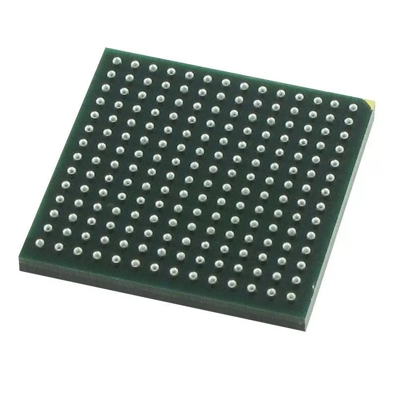

TPS7B8650BQDDARQ1
Brand: Texas Instruments
Texas Instruments TPS7B8650BQDDARQ1 is a power management component designed for AI Servers & Low-Altitude Economy (Drone and UAV) and related applications. In stock at Superb Automation — request a quote for competitive pricing and fast delivery.
Product Specifications
TPS7B8650BQDDARQ1
Texas Instruments — Power Management & Signal Chain
Product Overview
The TPS7B8650BQDDARQ1 from Texas Instruments is a power management / signal chain IC delivering high efficiency, precision regulation, and robust protection. Texas Instruments (TI) is a global leader in analog ICs, power management solutions, and embedded processors.
Superb Automation partners with leading brands including Qorvo, TI, ADI, XILINX, NVIDIA, Intel, ST, MACOM, Renesas, and Coilcraft to provide complete BOM and supply-chain solutions.
Key Features
- High-efficiency power conversion with low quiescent current
- Wide input voltage range with precision output regulation
- Integrated over-current, over-temperature, and short-circuit protection
- Small footprint packaging for space-constrained designs
- AEC-Q100 qualified options available for automotive applications
- Flexible sequencing and soft-start control
Key Specifications
| Input Voltage | V |
| Output Voltage | V |
| Output Current | A |
| Switching Frequency | kHz |
| Efficiency | % |
| Quiescent Current | µA |
| Topology | — |
| Package | — |
| Operating Temp | °C |
| Protection | — |
Applications
Industrial Automation
Automotive Electronics
Telecom Infrastructure
Server & Data Center Power
Medical Devices
Consumer Electronics
Request Quote — In Stock, 100% New & Original, Full Warranty
TPS7B8650BQDDARQ1: 5 V at 500 mA with a power-good pin in the B body
The TPS7B8650BQDDARQ1 is a 500 mA automotive regulator with a fixed 5 V output, a 3 V to 40 V input range and 17 uA of quiescent current at light load. The B in the order code is not decoration: it marks the DDA eight pin HSOIC version that brings the power-good pin out on pin 6, where the base DDA row has no PG pin at all. A board that needs a rail monitor therefore has to name the B code, and a board that does not should not pay for it.
Accuracy is plus or minus 0.85 percent over line, load and temperature, which is the tightest in this part of the 40 V family, and the power-good delay is set by a capacitor on the DELAY pin so a supervisor can wait for the rail to settle before releasing a processor. Dropout is 464 mV typical and 630 mV maximum at 500 mA into 3.3 V, the feedback reference is 0.656 V, and the adjustable rows of the same family take the output from 1.2 V to 18 V.
Key electrical data for the 500 mA part
| Input range | 3 V to 40 V, 42 V maximum, load dump tolerant |
| Output | 5.0 V fixed at plus or minus 0.85 percent over line, load and temperature |
| Output current | 500 mA, current limit 540 mA to 780 mA |
| Quiescent current | 17 uA typical at light load, which suits an always-on module |
| Dropout | 464 mV typical and 630 mV maximum at 500 mA into a 3.3 V rail |
| Power good | rising threshold 95 percent, falling 93 percent, with 2 percent of hysteresis |
| Delay | set by a capacitor on the DELAY pin, from microseconds to hundreds of milliseconds |
Package, marking and reel data
| Body | HSOIC DDA, 8 pins with a thermal pad, 2500 pieces per reel |
| Finish and moisture | SN, level 3, 260 C peak reflow, 168 hour floor life |
| Marking | B8650B |
| Grade | AEC-Q100 with a junction range of minus 40 to 150 C |
| Pin out | PG on pin 6, DELAY on pin 3, FB or NC on pin 2 depending on the row |
Where the B body is the right B body
A 500 mA rail at 5 V in a vehicle usually feeds a display, a camera module or a cluster segment, and all three want to know when the rail is actually good before the processor starts. That is what the PG pin in the B body provides, and the DELAY capacitor turns it into a sequenced start instead of a race between two rails. The same regulator in the KVU body covers the case where the thermal path matters more than the monitor.
At 500 mA from 13.5 V into 5 V the part burns 4.25 W, which is beyond what an eight pin HSOIC can pass without real copper. The pad and the board are the whole story at that operating point, and a build that ignores them will hit thermal shutdown before it hits its load. Where the drop is that large, the honest answer is a switching stage in front and this part as a post regulator for the noise sensitive half of the load. The 0.85 percent window then applies only to the part of the rail that still needs it, and the coarse section can live with a wider tolerance that costs nothing.
Buyer questions on the TPS7B8650BQDDARQ1
How do the B and D rows of the DDA body differ? Both are eight pin HSOIC with a thermal pad and both carry the power-good function, and they differ in the pin assignment of the NC and PG pins. The order code has to match the land pattern, not just the voltage.
What is the default power-good threshold? The output is flagged good at 95 percent of nominal on the way up and 93 percent on the way down, with 2 percent of hysteresis. The DELAY pin only changes when the flag is released, not the threshold.
Can the 5 V point be adjusted? Not on this code. The adjustable rows of the TPS7B86-Q1 family take the output from 1.2 V to 18 V with an external divider and share the body, so a board can be built once and strapped either way.
Buying this regulator through a component supplier
An eight pin HSOIC with a PG pin is one line among twenty on an automotive board, and the qualification work is already done by the time production starts. Our date code management page covers the freshness rule on a level 3 part with a 168 hour floor life, which is the detail that catches most lines out. To compare the DDA and KVU bodies, power management cross reference lists both with their thermal figures.