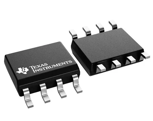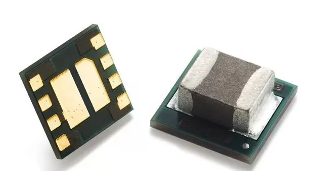

TPS25730DREFR
Brand: Texas Instruments
Texas Instruments TPS25730DREFR is a power management component designed for AI Servers & Low-Altitude Economy (Drone and UAV) and related applications. In stock at Superb Automation — request a quote for competitive pricing and fast delivery.
Product Specifications
TPS25730DREFR
Texas Instruments — Power Management & Signal Chain
Product Overview
The TPS25730DREFR from Texas Instruments is a power management / signal chain IC delivering high efficiency, precision regulation, and robust protection. Texas Instruments (TI) is a global leader in analog ICs, power management solutions, and embedded processors.
Superb Automation partners with leading brands including Qorvo, TI, ADI, XILINX, NVIDIA, Intel, ST, MACOM, Renesas, and Coilcraft to provide complete BOM and supply-chain solutions.
Key Features
- High-efficiency power conversion with low quiescent current
- Wide input voltage range with precision output regulation
- Integrated over-current, over-temperature, and short-circuit protection
- Small footprint packaging for space-constrained designs
- AEC-Q100 qualified options available for automotive applications
- Flexible sequencing and soft-start control
Key Specifications
| Input Voltage | V |
| Output Voltage | V |
| Output Current | A |
| Switching Frequency | kHz |
| Efficiency | % |
| Quiescent Current | µA |
| Topology | — |
| Package | — |
| Operating Temp | °C |
| Protection | — |
Applications
Industrial Automation
Automotive Electronics
Telecom Infrastructure
Server & Data Center Power
Medical Devices
Consumer Electronics
Request Quote — In Stock, 100% New & Original, Full Warranty
TPS25730DREFR USB Type-C and USB PD sink controller with an integrated 7 A high voltage switch
The TPS25730D is a USB Type-C and USB Power Delivery controller for the sink side of a port, meaning the side that receives power. It handles the configuration channel signalling, the power delivery negotiation and the protection of the VBUS path, and it does so without firmware in the host, since the port behaviour is set by resistor straps on the configuration pins.
The D member integrates the high voltage switch on the power path, which is the difference from the S member that drives an external FET instead. The integrated switch is a 16 milliohm path at 25 degrees, rated for 7 A, with a soft start slew rate and a fast overvoltage response that turns the path off in a few microseconds when the source misbehaves.
Key parameters taken from the TPS25730DREFR document
| Supply | 3.0 V to 3.6 V on the 3.3 V rail, which is the controller supply and not the power path |
| VBUS range | 4 V to 22 V on VBUS, VBUS_IN and the power path |
| Switch path | Integrated PPHV switch on the D member, 16 milliohm typical and 19 milliohm maximum at 25 degrees with 6.5 A |
| Switch at temperature | 24 milliohm typical and 29 milliohm maximum at 125 degrees, 27 milliohm typical and 32 milliohm maximum at 150 degrees |
| Path current | 7 A rating on the integrated switch |
| Reverse comparison | 2 mV minimum, 6 mV typical and 10 mV maximum threshold, which is the comparator that decides the direction of current |
| Soft start | 2.8 V per millisecond minimum, 3.3 typical and 3.8 maximum on the gate of the external path |
| Overvoltage response | The switch is disabled within 2 to 4 microseconds of the comparator crossing |
| Normal shutdown | 400 to 1000 microseconds to disable the switch when the input falls below the output |
| ESD | 1000 V human body model and 500 V charged device model on all pins |
| LDO outputs | 1 mA from the 3.3 V LDO and 5 mA from the VBUS LDO |
| Configuration | Resistor straps on the configuration pins, with no firmware required in the host |
| Interfaces | I2C, GPIOs and ADC inputs for system monitoring |
| Package | WQFN of 38 pins |
| Carrier | 3000 pieces on a large reel |
| Moisture | Level 2 at 260 degrees with a one year floor life |
| Part marking | 25730D |
| Temperature | Minus 40 to plus 125 degrees, with the power path junction allowed to 150 degrees |
Every row above is read from the vendor document, not from a distributor summary. Where a window is printed, the window is what a production test should use, and the typical value is only a starting point for a first article.
Where the numbers matter in a real build
The two members of this family are not interchangeable on a board. The D member integrates the switch and brings the current through the package, while the S member drives a gate and expects an external FET. A board built for one will not work with the other, and the pin functions differ even though the pin count and the body are close. The device comparison table in the document is the only safe reference.
The reverse comparison threshold of 6 mV typical is what decides when the port stops accepting current and starts blocking it. A threshold that is too low would trip on noise; too high and the port keeps sinking current from a source that has already collapsed. The 2 mV to 10 mV window is tight on purpose, and the comparator response is measured in microseconds because a hot unplug can put the full cable inductance behind the event.
The soft start slew rate is set by the gate capacitor on the external path and is specified from 10 to 90 per cent of the final value. A slow slew keeps the inrush into the load capacitance low, and a fast slew keeps the port from sitting at an intermediate voltage for too long. The printed window of 2.8 to 3.8 V per millisecond is the range where the internal circuit behaves as specified, and a capacitor outside that range changes the behaviour without appearing in any table.
The integrated switch at 16 milliohm gives 0.78 W at 7 A, which is why the power path junction is allowed to 150 degrees while the controller itself is limited to 125. The thermal pad is the only path out of the package, and a board that treats the pad as a signal ground rather than as a thermal ground will run the part far hotter than the datasheet curves suggest.
The strap configuration is what makes this part usable on a product with no firmware. The port capability, the current it will request and the behaviour on a dead battery are all set by resistors, so the bill of materials carries a few more resistors and no code. The trade is that a change in port behaviour means a board change, which is a decision to take early in a programme.
- The member, D or S, because the integrated switch and the gate driver versions have different pin functions and different external parts.
- The strap resistors, since the port behaviour is set in hardware and a wrong value changes what the port asks for.
- The gate capacitor on the external path, because the slew rate window is 2.8 to 3.8 V per millisecond.
- The thermal pad, which carries 0.78 W at 7 A and decides the junction temperature.
- The 3.3 V rail, which has to be present for the controller to run even when the port is unplugged.
- The reverse comparison behaviour, because a port that keeps sinking current from a collapsed source is a system level failure, not a port level one.
Which projects this part fits
This part fits monitors, docking stations, notebooks, point of sale terminals and any product that receives power over a Type-C cable at more than 15 W. It also fits battery powered equipment that has to negotiate a higher voltage from a charger instead of drawing a fixed 5 V, which is the case for anything with a fast charge requirement above 15 W.
Questions that come up before a purchase order is released
Does this part need firmware?
No. The port behaviour, including the voltage and current it requests, is set by resistor straps on the configuration pins. The I2C interface is for monitoring, not for the negotiation itself.
What is the difference between the D and the S member?
The D member integrates the high voltage switch, so the current flows through the package. The S member provides a gate drive for an external FET. The pin functions differ and the two are not interchangeable on one board.
How much current can the integrated switch carry?
The path is rated at 7 A, and the resistance is 19 milliohm maximum at 25 degrees and 29 milliohm maximum at 125 degrees. The 7 A figure is a package and junction rating, not a promise about the cable.
What happens on a hot unplug?
The reverse comparator crosses at 2 to 10 mV and the switch is disabled within 2 to 4 microseconds, which keeps the load capacitance from discharging back into the cable.
Is the ESD rating enough for a connector?
The part is rated at 1000 V human body model and 500 V charged device model, which is a device level rating. A connector that is exposed to the outside world still needs system level protection on VBUS and on the configuration channel pins.
Can the port work with no battery?
The controller runs from the 3.3 V rail and the port behaviour is set in hardware, so the port can negotiate as soon as that rail is present. The sequencing of that rail against VBUS is a system decision and has to be checked against the document.
How SUPERB handles this line
Type-C sink controllers are chosen on the power path and on the strap configuration, and both are fixed at the board level, so a wrong member or a wrong strap value is a respin rather than a firmware change. Our power management cross reference lists the devices this part is cross referenced against, our pin to pin cross reference explains how we check a replacement before it goes on a board, and our incoming inspection plan covers the inspection we apply to these controllers on arrival.