


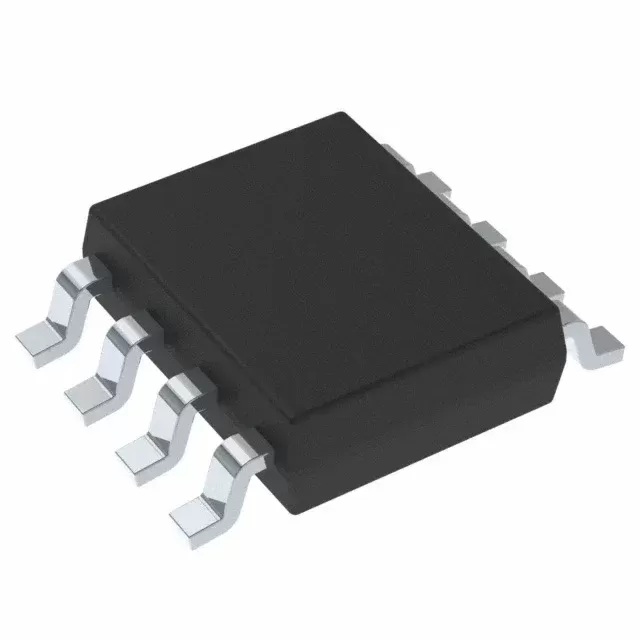

INA191A3IYFDR
Brand: Texas Instruments
Texas Instruments INA191A3IYFDR is a power management component designed for Industrial Automation and related applications. In stock at Superb Automation — request a quote for competitive pricing and fast delivery.
Product Specifications
INA191A3IYFDR
Texas Instruments — Power Management & Signal Chain
Product Overview
The INA191A3IYFDR from Texas Instruments is a power management / signal chain IC delivering high efficiency, precision regulation, and robust protection. Texas Instruments (TI) is a global leader in analog ICs, power management solutions, and embedded processors.
Superb Automation partners with leading brands including Qorvo, TI, ADI, XILINX, NVIDIA, Intel, ST, MACOM, Renesas, and Coilcraft to provide complete BOM and supply-chain solutions.
Key Features
- High-efficiency power conversion with low quiescent current
- Wide input voltage range with precision output regulation
- Integrated over-current, over-temperature, and short-circuit protection
- Small footprint packaging for space-constrained designs
- AEC-Q100 qualified options available for automotive applications
- Flexible sequencing and soft-start control
Key Specifications
| Input Voltage | V |
| Output Voltage | V |
| Output Current | A |
| Switching Frequency | kHz |
| Efficiency | % |
| Quiescent Current | µA |
| Topology | — |
| Package | — |
| Operating Temp | °C |
| Protection | — |
Applications
Industrial Automation
Automotive Electronics
Telecom Infrastructure
Server & Data Center Power
Medical Devices
Consumer Electronics
Request Quote — In Stock, 100% New & Original, Full Warranty
INA191A3IYFDR: a 100 V/V monitor with a hundred picoamps of bias
INA191A3IYFDR is the 100 V/V member of the INA191 family in a six ball DSBGA on a 3000 piece large reel. Its bias current is 100 picoamps typical, its offset is 12 microvolts maximum, its rejection is 132 dB minimum, and it draws 43 microamps with 100 nanoamps in shutdown, all in a body of 1.17 by 0.765 millimetres.
The part is one direction only: the reference node is not brought out on the six ball body, so the output starts near zero and rises with current. The bidirectional member of the same family is the INA2191 in a twelve ball body. A channel that measures a battery discharge, a charger output or a single rail load fits this part, and a channel that has to see reverse current does not.
INA191A3IYFDR as the vendor document publishes it
| Gain | 100 V/V fixed |
| Gain error | 0.04 per cent typical, 0.25 per cent maximum |
| Gain error drift | 2 ppm per degree typical, 7 maximum |
| Nonlinearity | 0.01 per cent typical of full scale |
| Offset voltage | 2.5 microvolts typical, 12 microvolts maximum, referred to the input |
| Offset drift | 10 nanovolts per degree typical, 130 maximum |
| Input bias current | 0.1 nanoamps typical, 3 nanoamps maximum |
| Input offset current | 70 picoamps typical |
| Common mode rejection | 132 dB minimum, 150 typical, over minus 40 to plus 125 degrees |
| Power supply rejection | 1 microvolt per volt typical, 5 maximum |
| Common mode range | minus 0.2 volts to plus 40 volts, independent of the supply |
| Supply range | 1.7 volts to 5.5 volts |
| Quiescent current | 43 microamps typical, 65 maximum when enabled |
| Shutdown current | 100 nanoamps maximum |
| Bandwidth | 35 kHz at this gain, 45 kHz at 25 V/V and 27 kHz at 500 V/V |
| Slew rate | 0.3 volts per microsecond |
| Settling to 1 per cent | 30 microseconds from a current step |
| Swing to the positive rail | 23 millivolts typical, 40 maximum into 10 kohm |
| Swing to ground | 0.05 millivolts typical, 1 maximum |
| Zero current output | 1 millivolt typical at this gain, 3 maximum |
| Direction | one direction only, no reference pin on the six ball body |
| Body | DSBGA, six ball, 1.17 by 0.765 millimetres |
| Temperature range | minus 40 to plus 125 degrees |
| Vendor status | active, 3000 piece large reel |
| Catalogue code | INA191A3IYFDR |
| Vendor string | INA191A3IYFDR |
| Body | DSBGA, YFD, six ball, 1.17 by 0.765 millimetres |
| Moisture level | level 1, 260 degrees, no floor life limit |
| Direction | one direction, no reference pin |
One hundred picoamps of bias in a body under one square millimetre
INA191A3IYFDR is a current shunt monitor with a 100 picoamp typical input bias current in a six ball DSBGA that measures 1.17 by 0.765 millimetres. The input window is minus 0.2 to plus 40 volts independent of the supply, the supply is 1.7 to 5.5 volts, and the quiescent current is 43 microamps with 100 nanoamps in shutdown.
The bias figure is the whole point. A 5 megaohm path with 100 picoamps across it sees 0.5 microvolts, and the same path with the 500 picoamps of the INA186 sees 2.5 microvolts, which is a sixth of that part's maximum offset. Microamp measurement through a large shunt is limited by bias current and by the amplifier's own offset in that order, and this part is the one in the family that pushes both terms down at once, in the body that fits under a camera module or inside a battery connector shell.
Twelve microvolts of offset and 130 nanovolts per degree
Offset on INA191A3IYFDR is 2.5 microvolts typical and 12 microvolts maximum referred to the input, with 10 and 130 nanovolts per degree of drift, and the supply rejection is 1 microvolt per volt typical and 5 maximum. The rejection of the input pair is 132 dB minimum over minus 40 to plus 125 degrees, the same figure the INA190 publishes.
The drift row is what separates a part that can be trimmed at test from one that cannot. Twelve microvolts of initial offset on a gain of 100 is 1.2 millivolts at the output and a single trim removes it; 130 nanovolts per degree over a 100 degree excursion adds 13 microvolts at the input, which on a 100 microvolt full scale is 13 per cent if it is left in. A channel that has to hold its calibration from a cold start to a hot soak needs the trim and the drift both, and the datasheet prints them separately for that reason.
One direction only, and the INA2191 that changes that
INA191A3IYFDR measures current in one direction. The reference node that would offset the output at zero current is not brought out on the six ball body, so the output sits at a few millivolts with no current and rises from there. The bidirectional member of the same family, the INA2191, brings the reference out on a twelve ball body and measures in both directions.
That is a functional difference and not a grade. A charger that only sources current, a load switch that only feeds a rail, and a battery that is only discharged in the product's life all work with a one direction part. A battery that is charged and discharged, a motor that reverses, or a bus that can be back fed needs the two direction member, and the board has to carry the larger body and the reference divider for it. Deciding this after the board is released costs a respin, so it belongs in the requirements list.
A quarter of one per cent of gain error from the 50 V/V option up
Gain error on INA191A3IYFDR is 0.04 per cent typical and 0.25 maximum on the 50, 100, 200 and 500 V/V options, and 0.17 and 0.35 on the 25 V/V option, with 2 and 7 ppm per degree of drift across the family. Bandwidth falls with the gain: 45 kHz at 25 V/V, 37 at 50, 35 at 100, 33 at 200 and 27 kHz at 500.
The 25 V/V option is the odd row and the reason is the internal divider. At unity scale the output stage's own error is not divided by the gain, so it appears in full, which is why the lowest gain carries the widest window rather than the narrowest. A channel that needs 0.25 per cent and has a choice of gain should therefore avoid the 25 V/V option, and a channel that needs 25 V/V should budget the 0.35 per cent rather than assume the family figure applies to all five.
Forty three microamps, and what the enable pin is for
INA191A3IYFDR draws 43 microamps typical and shuts down to 100 nanoamps maximum through the enable input. On a wearable or a battery instrument that reads current once a second, the average current is the product of the two, and the enable pin is the difference between a monitor that costs more than the circuit it watches and one that does not.
The cost of using it is settling. The output has to be allowed to reach its value after the enable, and the converter's own sample and hold has to charge from the amplifier's output, so the reading window starts after both. The enable threshold is a fraction of the supply with hysteresis, so a control line driven from a lower rail needs a level check rather than a direct connection. On a board that measures continuously the pin can be tied high and the shutdown row ignored, which is the simpler build and the one most boards take.
Where the smallest body decides the part
INA191A3IYFDR is chosen when the board has no room, and the arithmetic that follows is about what that space costs. The six ball body has no reference pin, so the measurement is one direction. It has an enable, so it can sleep. Its input and supply pads are close together, so the return path of the shunt has to be planned rather than assumed, and a Kelvin connection to the shunt is worth more here than on a larger body.
It is the wrong part when the channel needs both directions, when the current range needs more than one gain option on the same board, or when the thermal rise of a small body in still air matters. For those cases the family's larger members or the INA190 in the SOT-23 are the better buy. Our amplifier cross reference page covers the alternatives, and the traceability report page covers what has to travel with a DSBGA reel, since a ball array has no marking to read.
A picoamp input is bought for a large shunt, and the shunt is usually the larger part of the error budget at that point. Our amplifier cross reference page covers the family, and the traceability report page covers the reel record for a ball array with no marking.
Can this part measure reverse current? No. The six ball body has no reference pin, so the output cannot be offset and the reading stops at the zero current level.
What is the gain error at 100 V/V? 0.04 per cent typical and 0.25 per cent maximum, with 7 parts per million per degree of drift, which is the tighter window the family prints from the 50 V/V option up.