


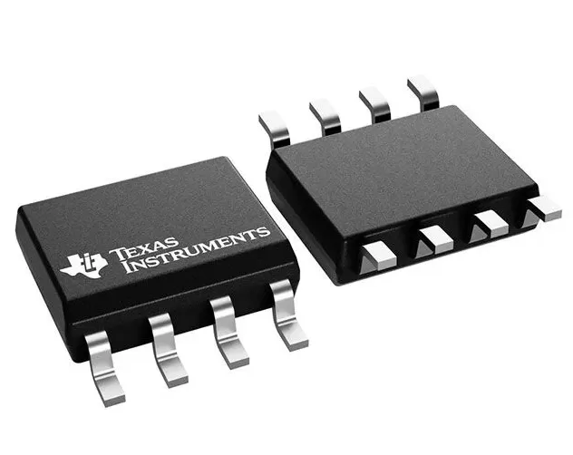

INA122P
Brand: Texas Instruments
Texas Instruments INA122P is a power management component designed for Industrial Automation and related applications. In stock at Superb Automation — request a quote for competitive pricing and fast delivery.
Product Specifications
INA122P
Texas Instruments — Power Management & Signal Chain
Product Overview
The INA122P from Texas Instruments is a power management / signal chain IC delivering high efficiency, precision regulation, and robust protection. Texas Instruments (TI) is a global leader in analog ICs, power management solutions, and embedded processors.
Superb Automation partners with leading brands including Qorvo, TI, ADI, XILINX, NVIDIA, Intel, ST, MACOM, Renesas, and Coilcraft to provide complete BOM and supply-chain solutions.
Key Features
- High-efficiency power conversion with low quiescent current
- Wide input voltage range with precision output regulation
- Integrated over-current, over-temperature, and short-circuit protection
- Small footprint packaging for space-constrained designs
- AEC-Q100 qualified options available for automotive applications
- Flexible sequencing and soft-start control
Key Specifications
| Input Voltage | V |
| Output Voltage | V |
| Output Current | A |
| Switching Frequency | kHz |
| Efficiency | % |
| Quiescent Current | µA |
| Topology | — |
| Package | — |
| Operating Temp | °C |
| Protection | — |
Applications
Industrial Automation
Automotive Electronics
Telecom Infrastructure
Server & Data Center Power
Medical Devices
Consumer Electronics
Request Quote — In Stock, 100% New & Original, Full Warranty
INA122P: a single supply instrumentation amplifier that draws 60 µA
The INA122 is a different animal from the bipolar instrumentation amplifiers around it. It runs from a single supply of 2.2 to 36 V, its output swings to within millivolts of both rails, and its quiescent current is 60 µA. The topology is two op amps rather than three, which is what makes the low supply current possible, and the price is paid in the input common mode range and in the noise floor: 60 nV per root Hz against 20 nV for a three op amp part of the same generation.
The P body is the eight pin plastic DIP, and the carrier is a 50 piece tube. A part that runs from 2.2 V and draws 60 µA belongs in a battery instrument, and the DIP body belongs in the prototype of that instrument, which is exactly the combination this row offers.
The INA122P rows as the addendum publishes them
| Part class | Single supply micropower instrumentation amplifier, two op amp |
| Vendor status | ACTIVE, production data |
| Data sheet | SBOS069B, revised December 2025 |
| Supply range | 2.2 V to 36 V, single or dual |
| Quiescent current | 60 µA |
| Output swing | Rail to rail |
| Gain equation | G = 5 + 200 kΩ divided by RG |
| Gain range | 5 to 10,000 V/V |
| Input offset voltage | 250 µV maximum |
| Offset drift | 3 µV per degree maximum |
| Input bias current | 25 nA maximum |
| Input noise | 60 nV per root Hz |
| Body | PDIP, P outline, 8 pins |
| Carrier | 50 pieces per tube |
| SOIC sibling | INA122U and INA122UA, 4.9 by 6 mm body |
| Moisture level | Not applicable to this package type |
| Temperature range | Minus 40 to plus 85 degrees |
| Reference pin | Pin 5, sets the output zero |
The gain range is the row that changes how the part is used. It starts at 5, not at 1, because the two op amp topology cannot be configured for unity gain: the first stage is a follower with a fixed divider, and the external resistor only sets the second stage gain above that floor. A channel that needs a gain of 1 or 2 cannot use this part, and that limitation is printed in the equation rather than in a note, which is why it is easy to miss.
Two op amps, rail to rail output and the common mode floor
The two op amp topology puts one amplifier in front as a follower and a second stage behind it as a difference amplifier. The input common mode range therefore includes the negative rail but comes close to the positive rail only when the output is low, and the classic failure is a signal that sits at the positive rail: the first stage cannot follow it and the output goes to the wrong rail. The vendor publishes the common mode range as a function of output voltage, and a single supply circuit has to be checked against that curve rather than against the headline rail to rail claim.
The rail to rail output is a genuine advantage in a 3 V system. A part that swings to within 100 mV of each rail gives back almost the whole supply as signal range, and on a 2.2 V minimum supply that matters: a bridge with a 20 mV full scale and a gain of 100 needs 2 V of swing, which is the entire supply. Engineers who use this part at 2.2 V are usually running a gain of 5 to 20 and a full scale of tens of millivolts, not hundreds.
60 µA and what it does to the rest of the budget
Sixty microamps is small enough that the amplifier is no longer the dominant load in a battery instrument. A microcontroller in sleep mode draws more, a reference draws more, and a boost converter's quiescent current is comparable. At that point the circuit decision moves from the amplifier to the system, and the amplifier's contribution to the power budget is a rounding error that is worth having but is not the reason to choose the part.
The reason to choose it is the combination: 2.2 V operation, rail to rail output, and 60 µA in one package. A discrete two op amp instrumentation amplifier built from two micropower amplifiers would draw more, occupy more board area and need matching resistors. The integrated part removes the matching problem, which is the part of a discrete build that nobody wants to own.
Offset, drift and the trim that is not needed
A 250 µV maximum offset with 3 µV per degree drift is not a precision specification by the standards of the bipolar parts in this catalogue, and it does not need to be. On a 2.5 V full scale at a gain of 10 the offset is 0.01 per cent, and the drift over 40 degrees is 120 µV, which is 0.005 per cent. The channel is limited by the sensor, not by the amplifier, and a trim network would add cost without changing the result.
Where the offset does matter is a high gain channel on a small signal. At a gain of 1000 a 250 µV offset becomes 250 mV at the output, which is a tenth of a 2.5 V range and needs a trim or an AC coupling. The REF pin is the tool: it sets the output zero, so a channel that AC couples can put the zero anywhere in the output range and use the full swing for the signal.
Buying INA122P
The DIP row is active in a 50 piece tube, and the SOIC siblings carry the same die for a reflow line. The choice between them at the prototype stage is one of convenience, and the choice at production is one of process. The grade question is smaller here than in a precision family, because the offset row is a maximum rather than a bin, but the A suffix in the SOIC body and the G4 rows still exist and are worth checking against the customer's approved vendor list.
The bigger question for a battery instrument is the supply. The part runs from 2.2 V, but a circuit that uses a 3.6 V lithium cell and a 2.5 V rail has to check the output swing against the load. Our medical device components page covers the supply and documentation requirements we usually see on portable instruments, and the amplifier cross reference page lists the two op amp families we compare.
The reference divider on a single supply
On a single supply the output zero is set by the reference pin, and the reference network is part of the signal path. A divider of two equal resistors across the supply puts the zero at mid rail, and its noise appears at the output multiplied by the gain. A 100 nF across the lower resistor filters the divider's thermal noise and its supply noise at the same time, and it costs one component that is often left off the bill of materials because it does not appear in the vendor's application circuit.
The divider current is the other decision. A 10 kΩ pair across 3 V draws 150 µA, which is two and a half times the amplifier's own supply current, and it is the load that decides the battery life rather than the amplifier. A 100 kΩ pair draws 15 µA and needs a larger capacitor for the same filtering, and the trade between the two is a system one rather than an amplifier one.
Questions that arrive with this part number
Whether the part can be used at unity gain is the first question, and it cannot: the minimum gain is 5. Whether it can run from a 3.3 V rail with a signal that goes to ground is the second, and it can only if the input common mode range allows it at the output level in use, which needs the vendor curve rather than an assumption. The third question is the reference pin: tying it to ground sets the zero at ground, and tying it to a mid rail shifts the whole output range up.
The fourth is about protection. This part does not carry the 40 V input protection of the bipolar families, so an external clamp is needed on any input that a user can touch. A series resistor and two diodes at the connector is the standard arrangement, and the resistor is chosen against the 25 nA bias current rather than against the fault current.