


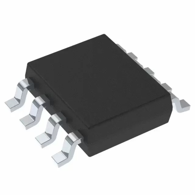

INA114AU
Brand: Texas Instruments
Texas Instruments INA114AU is a power management component designed for Industrial Automation and related applications. In stock at Superb Automation — request a quote for competitive pricing and fast delivery.
Product Specifications
INA114AU
Texas Instruments — Power Management & Signal Chain
Product Overview
The INA114AU from Texas Instruments is a power management / signal chain IC delivering high efficiency, precision regulation, and robust protection. Texas Instruments (TI) is a global leader in analog ICs, power management solutions, and embedded processors.
Superb Automation partners with leading brands including Qorvo, TI, ADI, XILINX, NVIDIA, Intel, ST, MACOM, Renesas, and Coilcraft to provide complete BOM and supply-chain solutions.
Key Features
- High-efficiency power conversion with low quiescent current
- Wide input voltage range with precision output regulation
- Integrated over-current, over-temperature, and short-circuit protection
- Small footprint packaging for space-constrained designs
- AEC-Q100 qualified options available for automotive applications
- Flexible sequencing and soft-start control
Key Specifications
| Input Voltage | V |
| Output Voltage | V |
| Output Current | A |
| Switching Frequency | kHz |
| Efficiency | % |
| Quiescent Current | µA |
| Topology | — |
| Package | — |
| Operating Temp | °C |
| Protection | — |
Applications
Industrial Automation
Automotive Electronics
Telecom Infrastructure
Server & Data Center Power
Medical Devices
Consumer Electronics
Request Quote — In Stock, 100% New & Original, Full Warranty
INA114AU: the precision instrumentation amplifier in a 16 pin SOIC
The INA114AU is the surface mount member of the INA114 family in the 16 pin wide body SOIC, with the same die, the same three amplifier topology and the same gain equation as the plastic DIP member. The specification that matters is unchanged: 50 µV of maximum offset at high gain, 0.3 µV per degree of drift, 2 nA of bias current, 115 dB of common mode rejection at a gain of 1000, and 40 V of input protection. The supply range starts at 2.25 V total and stops at 18 V.
What changes is the thermal path and the carrier. The SOIC body is 10.3 by 10.3 millimetres including pins and sits flat on the board, which is a better thermal connection than a plastic DIP in still air, and the carrier is a tube of 40 rather than 50. The reel version of the same body ships 1000 pieces under the slash one K string, and the moisture level on the reel row is level 3 with a 168 hour floor life.
The INA114AU rows as the addendum publishes them
| Part class | Three amplifier instrumentation amplifier, precision |
| Vendor status | ACTIVE, production data |
| Data sheet | SBOS014B, revised January 2026 |
| Gain equation | G = 1 + 50 kΩ divided by RG |
| Gain range | 1 to 10,000 V/V |
| Input offset voltage | 50 µV maximum at high gain |
| Offset drift | 0.3 µV per degree maximum at high gain |
| Input bias current | 2 nA maximum |
| Common mode rejection at G = 1000 | 115 dB minimum |
| Input overvoltage protection | 40 V without damage |
| Supply range | 2.25 V to 18 V total |
| Body | SOIC, DW outline, 16 pins, 10.3 by 10.3 millimetres |
| Carrier, tube row | 40 pieces in a tube |
| Carrier, reel row | 1000 pieces on a large tape and reel, printed with a slash before the one K |
| RoHS, tube row | Yes |
| Lead finish | Nickel palladium gold |
| Moisture level, tube row | Not applicable to this package type |
| Moisture level, reel row | Level 3 at 260 degrees, 168 hour floor life |
| Temperature range | Minus 40 to plus 85 degrees |
| Part marking | INA114AU |
| Revision row | INA114AU.B, same body and quantity |
| Status of both rows | Active, production data |
The temperature column on one of the revision rows in this family prints a dash instead of a range, which is a typesetting artefact of the addendum rather than a change in rating. The device is specified over minus 40 to plus 85 in the data sheet, and a customer who reads the dash as a gap will ask a question that has a one line answer.
Sixteen pins and a shorter return path
The DW body uses eight functional pins out of sixteen, and the extra spacing changes two things that matter on a precision part. The first is the leakage path between the two inputs, which is longer, and against a 2 nA bias current specification a longer path is worth having on a humid board. The second is the ground return: the reference pin can be routed on the same layer as the input with a ground plane underneath, which keeps the loop area small and the thermal EMF low.
The package also runs cooler than the DIP for the same dissipation, because the leads sit on copper rather than in air. On a part that draws a few milliamps and drives a load, the junction temperature rise is what sets the drift seen on the bench, and a 20 degree reduction in rise is 6 µV of offset drift at 0.3 µV per degree. That is the same order as the untrimmed offset of the part, which is why the package matters on a low level channel.
The gain resistor at high gain in a surface mount body
At a gain of 1000 the gain resistor is about 50 Ω, and in a surface mount build that value is physically small enough that a 0402 part is possible and a 0603 is easier to handle. The trace from the resistor to the RG pins should be a short wide pair, and the two resistors of a differential gain network should be placed symmetrically so the thermal gradients match. A 50 Ω resistor with 20 nH of loop inductance is a 0.25 Ω reactance at 2 MHz, which is small, and the same resistor with 200 nH of loop is not small at all.
A 0.1 per cent resistor at 50 Ω is a real part with a real temperature coefficient, and the price is not the issue; the availability is. A customer who specifies 0.05 per cent on a 50 Ω value should confirm the lead time before the board is released, because the part may be a special order while the amplifier is on the shelf.
Supply decoupling and the reference node
The reference pin is the one node that can quietly ruin a precision channel. It has to be driven from a low impedance, and a 10 kΩ divider with a 100 nF capacitor looks like a low impedance at DC and a 10 kΩ source at the frequencies where the amplifier's loop gain is falling. The right arrangement is a buffer or a reference device with a capacitor at the pin, and the capacitor should be a ceramic part with a stable dielectric rather than a high value electrolytic.
The supply decoupling follows the usual rule: 100 nF per rail at the pin and a 10 µF bulk part within a few centimetres. On a board with a switching converter, the bulk part should be on the analogue side of the filter, and the trace from the converter should not share the return with the reference pin.
Buying INA114AU
The tube of 40 is the practical carrier for a build of a few hundred boards, and the reel is the answer above that. Both are active, the finish is the same, and the die is shared with the plastic DIP and with the B bin, so a customer can trade package and grade independently. That flexibility is the reason this family has survived in medical and industrial instruments while newer parts have appeared.
The one thing to check on a purchase order is the string form. The reel is printed with a slash before the one K, and a system that strips the slash will produce a string that the vendor does not recognise. The tube string is the plain one and is what most orders use.
Questions that arrive with this part number
Whether the AU is drop in for the AP is the first question, and the answer is no, because the pin out and the body differ. Whether the reel row carries the same die as the tube is the second, and the answer is yes. Whether the part can drive a 10 kΩ load to within 100 mV of the rail is the third, and the answer is no, because the output stage needs headroom.
The fourth is whether the part is suitable for a 3.3 V single supply board. It runs at 3.3 V, but the output cannot reach the rails, so a full scale converter channel needs a reference and a headroom budget rather than a rail to rail assumption.
For a customer replacing a discontinued instrumentation amplifier with this body, our amplifier cross reference page lists the parameters that must match, and the drop in verification page sets out the tests to run on the first article.
The four unused pins are worth using as a fence on a mixed signal board. A guard trace tied to the reference and carried on the two spare pins between the inputs and the supply reduces the coupling from a nearby digital bus into the input pair, and it costs nothing to include in the footprint. On a channel measuring tens of millivolts, that coupling is often the difference between a quiet board and one that shows a step at every clock edge.