


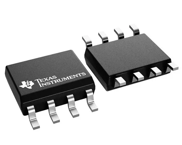

INA111BU
Brand: Texas Instruments
Texas Instruments INA111BU is a power management component designed for Industrial Automation and related applications. In stock at Superb Automation — request a quote for competitive pricing and fast delivery.
Product Specifications
INA111BU
Texas Instruments — Power Management & Signal Chain
Product Overview
The INA111BU from Texas Instruments is a power management / signal chain IC delivering high efficiency, precision regulation, and robust protection. Texas Instruments (TI) is a global leader in analog ICs, power management solutions, and embedded processors.
Superb Automation partners with leading brands including Qorvo, TI, ADI, XILINX, NVIDIA, Intel, ST, MACOM, Renesas, and Coilcraft to provide complete BOM and supply-chain solutions.
Key Features
- High-efficiency power conversion with low quiescent current
- Wide input voltage range with precision output regulation
- Integrated over-current, over-temperature, and short-circuit protection
- Small footprint packaging for space-constrained designs
- AEC-Q100 qualified options available for automotive applications
- Flexible sequencing and soft-start control
Key Specifications
| Input Voltage | V |
| Output Voltage | V |
| Output Current | A |
| Switching Frequency | kHz |
| Efficiency | % |
| Quiescent Current | µA |
| Topology | — |
| Package | — |
| Operating Temp | °C |
| Protection | — |
Applications
Industrial Automation
Automotive Electronics
Telecom Infrastructure
Server & Data Center Power
Medical Devices
Consumer Electronics
Request Quote — In Stock, 100% New & Original, Full Warranty
INA111BU: the B grade FET input amplifier in a 16 pin SOIC
The INA111BU combines the tighter offset bin of the INA111 family with the 16 pin wide body SOIC, which is the combination a board wants when it needs both a small package and a channel that is accurate without a trim. The electrical behaviour is the family behaviour: current feedback, 2 MHz at a gain of 10, 4 microseconds to 0.01 per cent at a gain of 100, 20 pA maximum bias current, 106 dB of common mode rejection at a gain of 100, and a gain equation of 1 plus 50 kΩ over RG.
The body is the DW outline at 10.3 by 10.3 millimetres with 16 pins, of which eight are used. The carrier is a tube of 40, and the same body with the same bin ships 1000 pieces on a reel under a separate string. The temperature range is minus 40 to plus 85 degrees, which is the whole family's range regardless of grade.
The INA111BU rows as the addendum publishes them
| Part class | FET input instrumentation amplifier, B grade offset bin |
| Vendor status | ACTIVE, production data |
| Data sheet | SBOS015, March 1998 |
| Gain equation | G = 1 + 50 kΩ divided by RG |
| Gain range | 1 to over 1000 V/V |
| Input bias current | 20 pA maximum |
| Offset drift | 5 µV per degree maximum |
| Common mode rejection at G = 100 | 106 dB minimum |
| Bandwidth at G = 10 | 2 MHz |
| Bandwidth at G = 100 | 450 kHz |
| Settling to 0.01 per cent | 4 µs at G = 100 |
| Gain error at G = 100 | 0.15 per cent typical, 0.7 per cent maximum |
| Nonlinearity at G = 100 | 0.001 per cent typical of full scale |
| Quiescent current | 3.3 mA typical, 4.5 mA maximum |
| Supply range | 6 V to 18 V |
| Output swing | 11 V minimum at 5 mA |
| Capacitive load stability | 1000 pF |
| Body | SOIC, DW outline, 16 pins |
| Carrier, tube row | 40 pieces in a tube |
| Carrier, reel row | 1000 pieces on a large tape and reel under the separate one K string |
| Lead finish | Nickel palladium gold |
| Moisture level, tube row | Not applicable to this package type |
| Moisture level, reel row | Level 3 at 260 degrees, 168 hour floor life |
| Temperature range | Minus 40 to plus 85 degrees |
| Part marking | INA111BU |
The temperature column on the reel rows of this family reads a dash rather than a range on one of the two rows, which is the vendor's way of saying the row inherits the range from the adjacent entry. It is not a statement that the part has no rating, and a customer who reads the dash as a gap in the specification is reading a formatting artefact rather than a limit.
Grade, package and the cost of a calibration
The B bin exists because the A bin is not enough for a channel that is accurate at low signal levels without a trim. On a 10 mV full scale with a 1 per cent target the budget is 100 µV, and the drift term alone is 200 µV over 40 degrees at 5 µV per degree. That arithmetic shows the limit of any grade of this family: the drift, not the initial offset, is what breaks a low level channel over temperature, and the fix is either a chopper stabilised part or a trim at the temperature of use.
Where the channel is trimmed at test, the A grade is the cheaper route and the B premium buys nothing. Where the channel is trimmed at 25 degrees and then expected to hold, the B grade buys a smaller starting error but not a smaller drift. The distinction is worth making in a quotation, because customers often ask for the B grade expecting it to fix a drift problem it cannot fix.
The four unused pins on a mixed signal board
The extra pins on the DW body are no connects, and they are useful as a fence. On a board where the input cable enters next to a digital bus, the two spare pins between the input and the supply can carry a guard trace tied to the reference, which reduces the coupling from the bus into the input. That is a small gain but it is free, and it costs nothing to include in a footprint.
The same pins are a trap if a board is copied from a dual amplifier footprint. A resistor fitted to what looks like the second channel's feedback pin will do nothing at best and inject current into an internal node at worst. The pin map in the data sheet is the only authority here, and the mechanical drawing does not show which pins are functional.
Power supply rejection at low frequency
The family is specified with a power supply rejection figure that is expressed per volt of supply change, scaled by gain, which is the honest way to publish it. At unity gain a 1 V change on the rail produces a few microvolts at the output; at a gain of 100 the same change is a hundred times smaller at the input but the same at the output, because the rejection is referred to the input. A customer regulating a 15 V rail to 1 per cent and expecting 100 µV of output noise from the supply is expecting the wrong thing.
The practical answer is a clean analogue rail. A 10 µF and a 100 nF at the part, fed from a separate regulator rather than from the digital 15 V, is worth more than any rejection figure. On a board with a switching converter, the switching frequency and its harmonics are what the rejection has to attenuate, and the rejection falls with frequency, so a 500 kHz converter is worse than a 100 kHz one for the same ripple.
Buying INA111BU
Two carriers, one die, and a grade that is worth paying for only on an untrimmed low level channel. The tube of 40 is the practical quantity for a build of a few hundred boards, and the 1000 piece reel is the answer above that. Both are active, and the finish is nickel palladium gold across the family, so a customer can move between the DIP and the SOIC without a finish question.
The string on this page is the tube row. A purchase order that quotes the slash one K form will be filled from the reel row, which carries a moisture level and a floor life that the tube does not, so the receiving inspection has to know which carrier was ordered before it opens the package.
Questions that arrive with this part number
Whether the BU is pin compatible with the AU is the first question, and the answer is yes, because the grade changes the trim and not the pin out. Whether it is compatible with the eight pin DIP is the second, and the answer is no. Whether the part can be used as a single supply amplifier is the third, and the answer is that 6 V is the floor, so a 5 V system needs a different family.
The fourth question is about the four unused pins: they can be grounded or left open, and grounding them is the better choice on a noisy board because it removes a floating node from the package.
For a customer comparing this bin against a modern low noise part, our amplifier cross reference page sets out the parameters that have to match, and the BOM sourcing page explains how a mixed order of tubes and reels is consolidated before shipment.
The temperature column on the tube row reads a range while the lead finish column reads a dash, which is the vendor's way of leaving the finish to the assembly site. A build that has a finish restriction should ask for the revision row rather than assume the dash means the same finish as the neighbouring rows.