


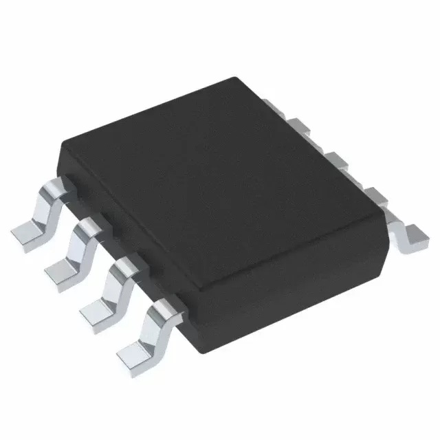

INA101HP
Brand: Texas Instruments
Texas Instruments INA101HP is a power management component designed for Industrial Automation and related applications. In stock at Superb Automation — request a quote for competitive pricing and fast delivery.
Product Specifications
INA101HP
Texas Instruments — Power Management & Signal Chain
Product Overview
The INA101HP from Texas Instruments is a power management / signal chain IC delivering high efficiency, precision regulation, and robust protection. Texas Instruments (TI) is a global leader in analog ICs, power management solutions, and embedded processors.
Superb Automation partners with leading brands including Qorvo, TI, ADI, XILINX, NVIDIA, Intel, ST, MACOM, Renesas, and Coilcraft to provide complete BOM and supply-chain solutions.
Key Features
- High-efficiency power conversion with low quiescent current
- Wide input voltage range with precision output regulation
- Integrated over-current, over-temperature, and short-circuit protection
- Small footprint packaging for space-constrained designs
- AEC-Q100 qualified options available for automotive applications
- Flexible sequencing and soft-start control
Key Specifications
| Input Voltage | V |
| Output Voltage | V |
| Output Current | A |
| Switching Frequency | kHz |
| Efficiency | % |
| Quiescent Current | µA |
| Topology | — |
| Package | — |
| Operating Temp | °C |
| Protection | — |
Applications
Industrial Automation
Automotive Electronics
Telecom Infrastructure
Server & Data Center Power
Medical Devices
Consumer Electronics
Request Quote — In Stock, 100% New & Original, Full Warranty
INA101HP: a precision instrumentation amplifier in a plastic DIP
The INA101HP is a three op amp instrumentation amplifier with laser trimmed thin film resistors on the die, in a 14 pin plastic DIP, published ACTIVE in a 25 piece tube. It is the plastic package member of a family that also ships in ceramic DIP, in a 16 pin surface mount body and in a TO-100 metal can, and the grades differ in offset, drift and temperature range rather than in function. Gain is set by one external resistor from 1 to 1000, following the equation G equals 1 plus 40 kΩ divided by RG.
This is the part a customer reaches for when a bridge or a thermocouple has to be amplified with a known error budget, and the reason is the input stage: three op amps with a differential input impedance of 10^10 Ω in parallel with 3 pF, so a 1 kΩ source imbalance produces almost no common mode error. A single op amp difference circuit with four discrete resistors cannot do that, and the resistor matching it would need is the reason this part exists.
The INA101HP rows as the addendum publishes them
| Part class | Instrumentation amplifier, three op amp, resistor programmable gain |
| Vendor status | ACTIVE, production data |
| Data sheet | SBOS133, Burr-Brown PDS-454K, July 1998 |
| Gain range | 1 to 1000 |
| Gain equation | G equals 1 plus 40 kΩ divided by RG |
| Initial offset, this grade | 125 µV plus 450 µV divided by G, typical |
| Initial offset, maximum | 250 µV plus 900 µV divided by G |
| Offset drift, this grade | 2 µV per degree plus 20 µV per degree divided by G |
| Offset drift, ceramic grades | 0.25 µV per degree, the headline figure |
| Gain error, G equals 1 | 0.04 per cent typical, 0.1 per cent maximum |
| Gain drift, G equals 100 | 22 ppm per degree typical, 110 maximum |
| Nonlinearity | 0.002 per cent of full scale typical |
| Common mode rejection, G equals 100 | 100 dB minimum, 105 dB typical |
| Differential input impedance | 10^10 Ω in parallel with 3 pF |
| Input voltage range | Plus or minus 10 V linear, 12 V typical |
| Input noise at 1 kHz | 13 nV per root hertz at G equals 1000 |
| Bandwidth, G equals 1 | 300 kHz at 3 dB |
| Bandwidth, G equals 100 | 25 kHz at 3 dB |
| Bandwidth, G equals 1000 | 2.5 kHz at 3 dB |
| Slew rate | 0.2 V per microsecond minimum, 0.4 typical |
| Settling to 0.01 per cent, G equals 1 | 30 µs typical, 45 µs maximum |
| Settling to 0.01 per cent, G equals 1000 | 500 µs typical, 650 µs maximum |
| Output | Plus or minus 10 V at 5 mA, 10 mA available |
| Capacitive load | 1000 pF stable |
| Supply range | Plus or minus 5 V to plus or minus 20 V |
| Quiescent current | 6.7 mA typical, 8.5 mA maximum |
| Body | PDIP, 14 pins |
| Tube row | INA101HP, 25 pieces, tube, Active |
| Temperature, specified | Minus 25 to plus 85 degrees |
| Temperature, operating | Minus 55 to plus 125 degrees, the addendum figure |
The last two rows are the ones most often misread. The addendum states the operating range, which is minus 55 to plus 125, while the data sheet specifies the electrical limits over minus 25 to plus 85. A customer who reads only the addendum will believe the part is specified to 125 degrees and will be disappointed at the first temperature chamber run.
Why the grade matters more than the family name
The headline claims on the first page of this data sheet, 25 µV of offset and 0.25 µV per degree of drift, belong to the ceramic grades with the C or M suffix. The plastic and surface mount rows, which is what this page and the next one cover, are 125 µV plus 450 divided by G and 2 µV per degree. That is a factor of five on offset and eight on drift, and it changes which applications the part can serve: a 10 mV strain gauge bridge with 125 µV of offset has 1.25 per cent of error before anything else is counted.
Gain error is better behaved across the grades, because it comes from resistor matching rather than from amplifier offset. At a gain of 1 the error is 0.04 per cent typical, and the external gain resistor adds its own tolerance on top, which is why the data sheet notes that RG is usually the largest single error term. A 0.1 per cent resistor is worth more than the next grade up.
Choosing the gain resistor and the source
With the equation above, a gain of 100 needs 404 Ω, a gain of 1000 needs 40 Ω, and a gain of 10 needs 4.44 kΩ. The low values are the awkward ones, because 40 Ω of lead and trace resistance is a measurable fraction of the resistor, and the gain then depends on the board rather than on the part. Above a gain of 500 the placement of that one resistor, and its distance from the pins, becomes part of the gain accuracy.
The source impedance should be balanced between the two inputs. A 1 kΩ imbalance is the condition the common mode rejection is specified at, so the part tolerates it, but a 10 kΩ imbalance on one leg will convert common mode noise into differential signal and no amount of gain will remove it. In a thermocouple application the cold junction compensation usually provides the balancing resistor for free.
Noise, bandwidth and the settling trade
The 13 nV per root hertz at a gain of 1000 is the input referred noise density, and it is flat enough that the total noise over a 2.5 kHz bandwidth is around 0.65 µV rms. Against a 10 mV full scale signal that is under 0.01 per cent, which is why this part is used with thermocouples and strain gauges rather than with fast transients. At a gain of 1 the bandwidth rises to 300 kHz but the input referred noise stays the same, so the total noise over the wider band rises by the square root of the bandwidth ratio.
The settling time tells the control side of the story. At a gain of 1000 the part needs 500 µs to reach 0.01 per cent, so a multiplexed system scanning ten channels can update each channel about two hundred times a second. That is fine for temperature and too slow for vibration, which is the dividing line between this part and a faster amplifier with worse offset.
Buying INA101HP
The tube holds 25 pieces and is the only live carrier for this grade in the plastic body, so a small build buys tubes and a large build buys the surface mount part on a reel. The tube is through hole style packaging with no moisture sensitivity rating, which means no floor life limit and no bake, and that is a real advantage for a repair depot that opens a tube once a month.
The plastic DIP has a copper lead frame and the data sheet notes its thermal performance, but the package is still a 14 pin through hole part with a junction to ambient resistance that limits it to drives of a few milliamps. Driving a long cable directly from the output is the usual way to discover that limit.
Questions that arrive with this part number
The first is whether this grade can be replaced by the ceramic one, and the answer is yes in function and no in error budget, because the ceramic part is five times better on offset. The reverse substitution is the one that fails a specification review. The second is the difference between the HP and the KU rows: the same die in a plastic DIP and in a 16 pin surface mount body, with the same electrical grades and different thermal paths.
The third is whether the offset can be trimmed. It can, through the two offset null pins, and the trim range is wide enough to bring a 250 µV part inside 25 µV at room temperature. What the trim does not fix is the drift, so a trimmed part still moves 2 µV per degree.
For a programme that is comparing grades, the amplifier cross reference page lists the family rows, and the incoming inspection plan covers the marking check on tubes from different grades.