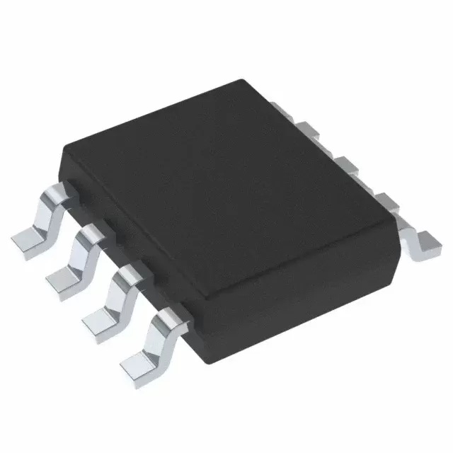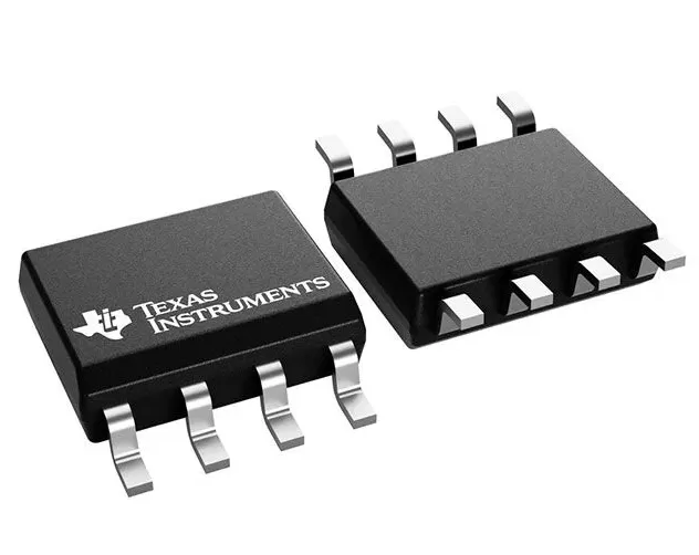

CD4016BM96
Brand: Texas Instruments
Texas Instruments CD4016BM96 is a power management component designed for Industrial Automation and related applications. In stock at Superb Automation — request a quote for competitive pricing and fast delivery.
Product Specifications
CD4016BM96
Texas Instruments — Power Management & Signal Chain
Product Overview
The CD4016BM96 from Texas Instruments is a power management / signal chain IC delivering high efficiency, precision regulation, and robust protection. Texas Instruments (TI) is a global leader in analog ICs, power management solutions, and embedded processors.
Superb Automation partners with leading brands including Qorvo, TI, ADI, XILINX, NVIDIA, Intel, ST, MACOM, Renesas, and Coilcraft to provide complete BOM and supply-chain solutions.
Key Features
- High-efficiency power conversion with low quiescent current
- Wide input voltage range with precision output regulation
- Integrated over-current, over-temperature, and short-circuit protection
- Small footprint packaging for space-constrained designs
- AEC-Q100 qualified options available for automotive applications
- Flexible sequencing and soft-start control
Key Specifications
| Input Voltage | V |
| Output Voltage | V |
| Output Current | A |
| Switching Frequency | kHz |
| Efficiency | % |
| Quiescent Current | µA |
| Topology | — |
| Package | — |
| Operating Temp | °C |
| Protection | — |
Applications
Industrial Automation
Automotive Electronics
Telecom Infrastructure
Server & Data Center Power
Medical Devices
Consumer Electronics
Request Quote — In Stock, 100% New & Original, Full Warranty
CD4016BM96: four bilateral switches in a 14-lead SOIC on a 2500 piece reel
CD4016BM96 is the tape and reel member of the CD4016B family, four independent bilateral switches in one body, otherwise known as a quad analogue switch. The vendor descriptor reads 20 V, 1:1 single pole single throw, four channels, analogue switch, with 100 pA of on-state leakage current, the document is the CD4016B data sheet revision E, and the parametric table gives four channels, a 40 MHz bandwidth, an operating supply set covering 3.3, 5, 12, 16 and 20 V, break-before-make switching and a minus 55 to plus 125 degree range. Each switch is a transmission gate with a control input, and the four are independent of one another.
The addendum lists CD4016BM96 as Active in production, SOIC (D) with 14 leads, 2500 pieces on a large tape and reel, RoHS yes with a nickel-palladium-gold finish, moisture sensitivity level 1 at a 260 degree peak, minus 55 to plus 125 degrees, and the marking CD4016BM. The important procurement detail on this row is that the tube member of the same body, CD4016BM, is Obsolete, as is CD4016BMT, so the 2500 piece reel is the only active surface mount format for this die in the addendum.
The CD4016BM96 row as the vendor addendum publishes it
| Part class | Quad bilateral switch, four independent transmission gates |
| Vendor descriptor | 20 V, 1:1 single pole single throw, four channels, 100 pA on-state leakage |
| Vendor document | CD4016B data sheet revision E |
| Channels | Four, each with its own control input |
| Bandwidth, parametric table | 40 MHz typical |
| Supply set in the parametric table | 3.3 V, 5 V, 12 V, 16 V and 20 V |
| Switching behaviour | Break before make |
| On-state leakage, vendor descriptor | 100 pA |
| Control input current, maximum | 1 microamp at 18 V |
| Parametric ratings | 5 V, 10 V and 15 V tables |
| Quiescent current | Tested to maximum at 20 V on every unit |
| Package for this code | SOIC (D), 14 leads |
| Packing | 2500 pieces on a large tape and reel |
| Lead finish | NIPDAU |
| Moisture level | Level 1, 260 degrees peak, unlimited floor life |
| Operating range | Minus 55 to plus 125 degrees |
| Status | Active, production |
| Part marking | CD4016BM |
| Tube member of the same body | CD4016BM, Obsolete, quantity blank |
| Other obsolete row | CD4016BMT, quantity blank, Call TI |
| Ceramic and DIP rows | CD4016BF and CD4016BE, 25 piece tube, still listed |
| On resistance in the vendor text | Not published as a text figure, the electrical table is a scan |
What a bilateral switch does that a logic gate cannot
A transmission gate passes a signal in both directions, so the same part can select between two sources, route a signal to two destinations, or break a path in a circuit that carries an analogue level rather than a logic state. In the 4016 the switch is controlled by a single input per channel, and the control input is a CMOS gate that draws only leakage, so one microcontroller pin can control a switch that passes a signal several volts away from the logic rail, provided the signal stays inside the supply rails of the switch.
The limitation is equally important. The switch is not a buffer, so the signal that comes out is the signal that went in, attenuated by the on resistance and loaded by whatever sits on the other side. A 4016 in series with a 10 k load and an on resistance of a few hundred ohms already loses a few per cent of level, and at 5 V the on resistance is higher than at 15 V, which is why the same circuit behaves differently on a 5 V rail and a 12 V rail. The vendor prints the on resistance in the electrical table, which on this document is a scanned image, so this page states the dependency and does not quote a figure it cannot read.
Bandwidth, leakage and the 20 V ceiling
The parametric table gives a 40 MHz bandwidth, which is high enough for audio, for a multiplexed sensor front end and for switching a low frequency clock, and low enough that the part is never chosen for a video or an RF path. The 100 pA on-state leakage in the vendor descriptor is the number that matters in a sample and hold circuit, because leakage through an open switch discharges a hold capacitor, and a 100 pA into 1 nF is 0.1 V per second, which sets the hold time almost exactly.
The 20 V ceiling is what separates this part from the 74HC4066 class. A 4066 stops at 6 V and is faster and lower resistance at 5 V; the 4016 goes to 20 V and behaves well in a 12 V or 15 V analogue chain where a 4066 cannot be used at all. The choice between them follows the rail, not the bandwidth.
Break before make, and the glitch it prevents
The parametric table lists break-before-make switching, which means the part opens one path before it closes the next. In a multiplexer built from two 4016 channels and an inverter, that behaviour prevents the moment when both sources are connected to the output at once, which would short two signals together through the on resistance of the two switches. The cost is a short interval when neither path is connected, so a circuit that cannot tolerate an open output needs a hold capacitor or a different topology.
Because the four channels are independent, a multiplexer built this way also needs the control signals to be complementary, and the inverter that generates the complement adds a delay of its own. A circuit that needs a clean two-to-one selection with guaranteed break before make takes a CD4053 instead, which has the inverter inside the package and the three changeover switches on one control pin.
Where the 4016 sits against the 4051 and the 4066
Inside the CD4000B family the analogue switch range runs from this quad single pole device through the CD4051B 8-channel multiplexer, the CD4052B differential 4-channel multiplexer and the CD4053B triple two-to-one switch. The 4016 is the one with four independent control inputs, which is the right choice when the four switches are unrelated, and the wrong choice when they are a multiplexer, because the 4051 brings the address decoder with it.
Against the 4066 the difference is the rail. The 4066 is the pin compatible part with a lower on resistance at 5 V and a 15 V ceiling; the 4016 goes to 20 V. A board that runs at 15 V can use either, and a board that runs at 18 V needs the 4016.
Incoming checks on an obsolete sibling and an active reel
The first check is the row itself, because CD4016BM and CD4016BMT are both obsolete and the active code is the 96 reel. A bag of tubes that claims to be 4016BM is either old stock or a repack, and the addendum gives no active tube row for the SOIC to compare it against. The second check is functional: each switch should be tested for on resistance in both directions at the rail the board uses, because a transmission gate can fail in one direction while passing in the other, and a simple continuity test will miss it.
The reference pages are the incoming inspection plan, the obsolete part cross reference hub for a replacement route on the obsolete tube code, and component obsolescence management when the board is in service and the switch has to be kept available.
Questions that come up on the 4016
Whether the switch passes a signal below the negative rail. It does not, because the body diode conducts and the switch stops behaving as a switch, so a bipolar signal needs a split supply or a different part.
Whether the four channels can be paralleled to lower the on resistance. They can, with the control inputs tied together, at the cost of more capacitance and a slower switch.
Whether the part can switch a 20 V signal on a 12 V supply. It cannot, because the signal has to stay inside the supply rails, and a 20 V signal needs a 20 V supply.
Whether the obsolete tube row can still be bought. It appears in the addendum with a blank quantity and a Call TI instruction, which means the vendor no longer supports it, and any stock is broker stock with the traceability risk that implies.