


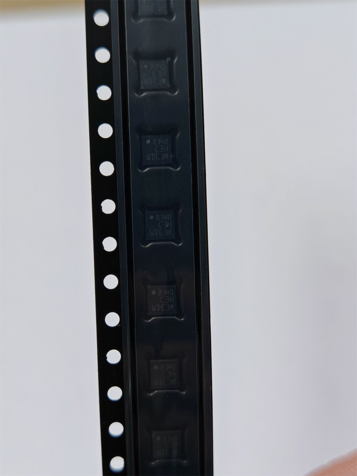

BQ25306RTER
Brand: Texas Instruments
Texas Instruments BQ25306RTER is a power management component designed for AI Servers & Low-Altitude Economy (Drone and UAV) and related applications. In stock at Superb Automation — request a quote for competitive pricing and fast delivery.
Product Specifications
BQ25306RTER
Texas Instruments — Power Management & Signal Chain
Product Overview
The BQ25306RTER from Texas Instruments is a power management / signal chain IC delivering high efficiency, precision regulation, and robust protection. Texas Instruments (TI) is a global leader in analog ICs, power management solutions, and embedded processors.
Superb Automation partners with leading brands including Qorvo, TI, ADI, XILINX, NVIDIA, Intel, ST, MACOM, Renesas, and Coilcraft to provide complete BOM and supply-chain solutions.
Key Features
- High-efficiency power conversion with low quiescent current
- Wide input voltage range with precision output regulation
- Integrated over-current, over-temperature, and short-circuit protection
- Small footprint packaging for space-constrained designs
- AEC-Q100 qualified options available for automotive applications
- Flexible sequencing and soft-start control
Key Specifications
| Input Voltage | V |
| Output Voltage | V |
| Output Current | A |
| Switching Frequency | kHz |
| Efficiency | % |
| Quiescent Current | µA |
| Topology | — |
| Package | — |
| Operating Temp | °C |
| Protection | — |
Applications
Industrial Automation
Automotive Electronics
Telecom Infrastructure
Server & Data Center Power
Medical Devices
Consumer Electronics
Request Quote — In Stock, 100% New & Original, Full Warranty
BQ25306RTER standalone seventeen volt three amp buck charger for one and two cell packs
The BQ25306RTER is a standalone buck charger that takes 4.1 V to 17 V in and pushes up to 3 A into a one cell or two cell pack. There is no bus and no register map: the charge voltage is set by a resistor divider, the charge current by a resistor, and the part starts charging when power is applied. That makes it the choice for products where a firmware team is not available to write a charger driver, or where the charger must work before the processor boots.
The converter runs at 1.2 MHz, which keeps the inductor small, and the FETs, the current sense, the loop compensation and the bootstrap diode are all inside a 3 mm by 3 mm QFN. Efficiency is quoted at 92.5 percent charging a one cell pack at 2 A from 5 V, 91.8 percent from 9 V, and 95 percent charging a two cell pack at 2 A from 12 V. Battery leakage in standby is 200 nA, which is what allows a product to sit in a box for a year and still have charge.
Key parameters taken from the BQ25306RTER document
| Function | standalone synchronous buck charger, 1 or 2 cells |
| Package | RTE, 16 pin WQFN, 3.00 mm by 3.00 mm |
| Input range | 4.1 V to 17 V operating, 28 V absolute maximum |
| Switching frequency | 1.2 MHz |
| Fast charge current | up to 3 A, plus or minus 10 percent regulation |
| Charge voltage | 3.4 V to 9.0 V, set by a divider as 1.1 V times one plus R1 over R2 |
| Charge voltage accuracy | plus or minus 0.5 percent |
| Precharge and termination | 10 percent of the fast charge current each |
| Battery leakage in standby | 200 nA at 4.5 V |
| Supply current with the charger disabled | 4.25 uA on the input |
| Thermal regulation | 120 C junction, with thermal shutdown above it |
| Input voltage regulation | tracks the battery, 1.044 times battery plus 0.125 V |
The table above is read from the vendor document rather than from a catalogue summary. Where the document prints a minimum and a maximum, both are kept, because the number a test station should use is the limit and not the typical.
Where the numbers matter in a real build
The charge voltage is set by a divider, not by a register, and the ratio is fixed at 1.1 V times one plus R1 over R2. That means the accuracy of the finished product depends on the two resistors as much as on the part. A 1 percent resistor pair is normal; a 5 percent pair moves the 4.2 V point by more than 20 mV, which is a real capacity loss over a pack life.
Input voltage regulation tracks the battery rather than sitting at a fixed floor. The threshold is 1.044 times the battery voltage plus 125 mV, so a deeply discharged pack pulls the input down with it and the charger reduces current instead of collapsing a weak adapter. Products running from a 12 V vehicle rail or a long cable benefit, because the drop on the cable is absorbed without a separate compensation circuit.
The 17 V input rating with 28 V absolute maximum is what allows the part to be used behind a barrel jack that might see an unregulated adapter. It is not a 24 V part: continuous operation above 17 V is outside the recommended range, and the guard is for transients, not for a wrong adapter left plugged in.
The 3 A rating holds only while the thermal path holds. In a 3 mm by 3 mm body with 1.2 MHz switching, the junction temperature rises quickly at 3 A into a 4.2 V pack from a 9 V input. Products that need 3 A continuously usually run the part at 2 A and take the efficiency, or they add copper and airflow. The thermal regulation at 120 C is a safe fold back, not a working point.
- No bus and no registers means the charger works on a bare board before any firmware exists, which shortens bring up.
- Reverse blocking is integrated, so a pack cannot discharge back into the input when the adapter is removed.
- The internal current sense removes the shunt and its error from the charge current path.
- The 200 nA standby leakage is low enough for products that ship with a charged pack and sit in storage.
Which projects this part fits
Wireless speakers, gaming accessories, cradle chargers, portable medical devices and any one or two cell product that charges from a 5 V, 9 V or 12 V adapter without a host controller. It also suits products that must charge from a vehicle rail, where the 17 V window and the tracking input regulation both help. Our power management cross reference lists the standalone chargers we hold, and the medical device component page covers the traceability needed for charger parts in medical builds.
Setting the divider and proving the charge point
The charge voltage comes from a divider and the equation printed in the document is 1.1 V times one plus R1 over R2, so the ratio is what matters and the absolute resistor values only set the divider current. The table gives three worked points at a 100 kOhm bottom resistor.
| Pack | Target charge voltage | R1 with R2 at 100 kOhm |
| 1 cell lithium ion | 4.20 V | 281.8 kOhm |
| 1 cell, 4.35 V chemistry | 4.35 V | 295.5 kOhm |
| 2 cell lithium ion | 8.40 V | 663.6 kOhm |
With 1 percent resistors the finished charge point moves by roughly 1 percent of the target, which is about 40 mV on a 4.2 V pack and 84 mV on a two cell pack. That is wider than the 0.5 percent accuracy of the part itself, so the resistor tolerance, not the charger, sets the accuracy of the product. A 0.1 percent pair is the usual choice when the customer's specification quotes the charge voltage to two decimal places.
The first article check measures the charge voltage at the pack terminals after termination, not at the charger output, because the current sense resistor and the protection FETs sit between the two. It also confirms the precharge and termination points, both of which are fixed at 10 percent of the fast charge current, and the input regulation behaviour with a lab supply set to sag under load. A board that passes the voltage check but folds back at 1 A is usually a divider that was calculated for a different bottom resistor than the one fitted.
Questions that come up before a purchase order is released
Can this charge a lithium iron phosphate pack?
Yes. The charge voltage is set by the divider across 3.4 V to 9.0 V, so a 3.6 V or 3.65 V iron phosphate pack is set the same way as a 4.2 V lithium ion pack. The termination and precharge ratios stay at 10 percent of the fast charge current, which suits most iron phosphate cells.
Why is the input regulation tied to the battery voltage?
It keeps the adapter out of current limit as the pack voltage rises. A fixed input floor that works at 3.0 V wastes headroom at 4.2 V; a tracking threshold follows the pack and uses the adapter fully at every point in the charge. The cost is that the threshold moves with the pack, so a supply that sags below it will simply reduce charge current.
What sets the 3 A limit in a real product?
Thermal rise in the actual enclosure and the adapter's current capability. The part folds back at 120 C junction, so a board that delivers 3 A on the bench may deliver 2 A in a sealed case. The 10 percent current accuracy also means a 3 A setting can read 2.7 A at the low end of the window, which matters when a charge time is quoted to a customer.
How SUPERB handles this line
We supply the BQ25306RTER with the divider and current set resistors calculated for the pack, and we can kit the inductor and the input and output capacitors so the converter arrives complete. If a product is moving from a linear charger, the adapter and the thermal path usually both change; send the adapter list and the enclosure drawing and we will check the 3 A claim against the real thermal path. Start with the drop in replacement check page.

