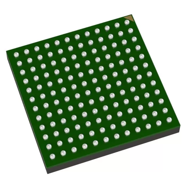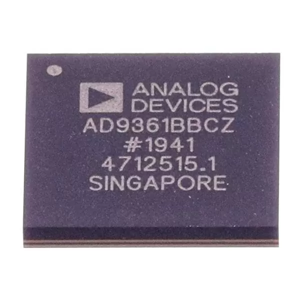

LTC1050CS8#TRPBF
Brand: Analog Devices
Analog Devices LTC1050CS8#TRPBF is a analog & mixed-signal component designed for Precision Instrumentation and related applications. In stock at Superb Automation — request a quote for competitive pricing and fast delivery.
Product Specifications
LTC1050CS8#TRPBF
Analog Devices — Analog & Mixed-Signal ICs
Product Overview
The LTC1050CS8#TRPBF from Analog Devices is a high-performance analog / mixed-signal IC providing precision signal acquisition, conversion, and conditioning. Analog Devices (ADI) is a world leader in high-performance analog, mixed-signal, and DSP ICs for instrumentation, healthcare, automotive, and communications.
Superb Automation partners with leading brands including Qorvo, TI, ADI, XILINX, NVIDIA, Intel, ST, MACOM, Renesas, and Coilcraft to provide complete BOM and supply-chain solutions.
Key Features
- High-resolution data conversion with excellent SNR and THD
- Wide dynamic range and high linearity across operating conditions
- Integrated voltage reference with low temperature drift
- Flexible digital interface — SPI, I2C, or parallel options
- Industrial/automotive temperature range with guaranteed specs
- Low power consumption with power-down modes
Key Specifications
| Resolution | bits |
| Channels | — |
| Sample Rate | kSPS |
| Interface | — |
| Supply Voltage | V |
| Operating Temp | °C |
| Package | — |
| INL | LSB |
| SNR | dB |
| THD | dB |
Applications
Precision Instrumentation
Industrial Process Control
Medical Imaging & Diagnostics
Automotive Sensor Interfaces
Communications Infrastructure
Test & Measurement
LTC1050CS8#TRPBF: 5 uV of Offset, 0.5 uV per Degree C, and No External Capacitors
The LTC1050CS8#TRPBF is a zero-drift operational amplifier with its chopping capacitors integrated on the die, so the two capacitors that a classic chopper amplifier needs on the board are simply not there. Maximum offset is 5 uV, maximum offset drift is 0.5 uV per degree C, low frequency noise is 1.6 uV peak to peak from 0.1 Hz to 10 Hz and is tested and guaranteed, minimum open loop gain is 130 dB, minimum power supply rejection is 125 dB, minimum common mode rejection is 120 dB, supply current is 1 mA, the supply range is 4.75 V to 16 V single, the input common mode range includes ground, the output swings to ground, gain bandwidth is 2.5 MHz, slew rate is 4 V per microsecond, and overload recovery is 1.5 ms from positive saturation and 3 ms from negative saturation. Pin 5 accepts an external clock for synchronisation.
The part is bought for DC accuracy in a single supply system where a bipolar precision amplifier would need a negative rail. A thermocouple, a strain gauge bridge or a shunt in a 12 V industrial product needs microvolt level offset and does not have room for a charge pump, and this is one of the few amplifiers that delivers both.
Half a microvolt per degree is twelve and a half times the offset over the full range
The headline offset is 5 uV and the guaranteed drift is 0.5 uV per degree C. Over 125 degrees of ambient swing that drift is 62.5 uV, twelve and a half times the offset the part was chosen for. The typical drift is 0.01 uV per degree C, which over the same span is 1.25 uV, so the difference between a typical part and a guaranteed part is fifty times the drift budget. A product that trims at room temperature and specifies accuracy over temperature has to work from the 0.5 uV figure, not the typical one, and at that point the offset trim is irrelevant and the drift is the whole error.
Noise integrates to 0.24 uV rms if the 1.6 uV peak to peak is taken at a crest factor of 6.6, which is 0.003 of a 16-bit bit on a 5 V span. The chopper therefore does not limit a 16-bit channel, and the term that does limit it is the drift, not the noise. At 24 bits the 0.24 uV rms is 0.8 of a bit on a 5 V span and the amplifier starts to matter.
| Offset | 5 uV maximum, 0.5 uV per degree C maximum drift |
| Drift over 125 C | 62.5 uV guaranteed, 12.5 times the offset, 1.25 uV typical |
| Low frequency noise | 1.6 uV peak to peak from 0.1 Hz to 10 Hz, 0.24 uV rms |
| Gain | 130 dB minimum, 160 dB typical, a ratio of 3.16 million |
| Rejection | 125 dB minimum PSRR, 120 dB minimum CMRR |
| Supply | 4.75 V to 16 V single, 1 mA, 5 mW at 5 V |
| Input range | Includes ground, output swings to ground |
| Speed | 2.5 MHz gain bandwidth, 4 V per microsecond, 637 kHz full power at 2 V peak to peak |
| Overload recovery | 1.5 ms from positive saturation, 3 ms from negative saturation |
| Package | 8-lead SOIC, also PDIP and metal can, external clock input on pin 5 |
Three milliseconds of overload recovery is a multiplexer problem
An amplifier that recovers from negative saturation in 3 ms cannot be used behind a multiplexer that switches at 1 kHz, because one overloaded channel blanks the next three samples. In a scanned thermocouple input the usual arrangement is a clamp on each channel so the amplifier never saturates, and the recovery time then never enters the budget. Where a clamp is not possible, the scan rate has to fall to a few hundred hertz, and that is a system level decision made by the recovery figure rather than by the bandwidth.
The integrated capacitors change behaviour in a second way that matters in a multi-channel instrument: without external capacitors there is no long lead carrying a switched node, so the chopper clock does not couple into neighbouring traces through the capacitor pins. Where several amplifiers share a board, pin 5 lets them run from one clock, which removes the beat note that appears when two free-running choppers operate a few hundred hertz apart and a slow scan samples first one and then the other.
Two questions buyers ask
Does it work on a 3.3 V rail?
No. The minimum supply is 4.75 V, which is the single most common mismatch for this part in a modern board. A 3.3 V system needs a different zero-drift amplifier with a 2.7 V minimum, and the available offset and drift in that class are usually similar while the noise is higher.
Can it replace a socket built for a general purpose precision amplifier?
It is offered as a plug-in replacement for most standard single op amps, with the same pinout and the same 8-lead footprint, and the electrical differences that matter are the 4.75 V minimum supply, the 1 mA supply current and the 3 ms overload recovery. A socket that fed the old part from a 5 V rail with a 10 kOhm load will work; a socket that ran it at 3 V or expected 100 us recovery will not.
Ordering and supply
The CS8 suffix is the 8-lead SOIC on the commercial temperature grade and the TRPBF suffix is tape and reel, lead free. The trap in this family is the drift grade and the package: the metal can and ceramic versions carry their own tables, and a commercial SOIC reel and an industrial part are not interchangeable on a specification even though the offset line on the first page is the same. Buying to the typical drift figure rather than the guaranteed one is the other common mistake, and it is invisible until the product is in a temperature chamber.
We hold and source this family for production and for repair. Start from the analog mixed signal ICs family page, compare a candidate against the amplifier cross reference, and where a zero-drift part has to go into an existing instrument, the sequence in how to verify a drop in replacement puts the supply minimum and the overload recovery ahead of the offset check.
Request Quote — In Stock, 100% New & Original, Full Warranty