


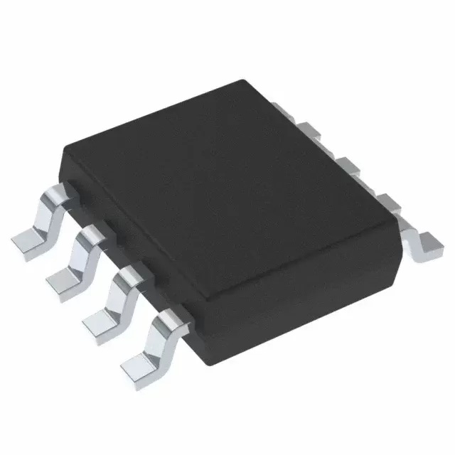

LF412CDR
Brand: Texas Instruments
Texas Instruments LF412CDR is a power management component designed for Industrial Automation and related applications. In stock at Superb Automation — request a quote for competitive pricing and fast delivery.
Product Specifications
LF412CDR
Texas Instruments — Power Management & Signal Chain
Product Overview
The LF412CDR from Texas Instruments is a power management / signal chain IC delivering high efficiency, precision regulation, and robust protection. Texas Instruments (TI) is a global leader in analog ICs, power management solutions, and embedded processors.
Superb Automation partners with leading brands including Qorvo, TI, ADI, XILINX, NVIDIA, Intel, ST, MACOM, Renesas, and Coilcraft to provide complete BOM and supply-chain solutions.
Key Features
- High-efficiency power conversion with low quiescent current
- Wide input voltage range with precision output regulation
- Integrated over-current, over-temperature, and short-circuit protection
- Small footprint packaging for space-constrained designs
- AEC-Q100 qualified options available for automotive applications
- Flexible sequencing and soft-start control
Key Specifications
| Input Voltage | V |
| Output Voltage | V |
| Output Current | A |
| Switching Frequency | kHz |
| Efficiency | % |
| Quiescent Current | µA |
| Topology | — |
| Package | — |
| Operating Temp | °C |
| Protection | — |
Applications
Industrial Automation
Automotive Electronics
Telecom Infrastructure
Server & Data Center Power
Medical Devices
Consumer Electronics
Request Quote — In Stock, 100% New & Original, Full Warranty
LF412CDR: the commercial grade of the JFET input dual on a reel
LF412CDR is the commercial grade of the dual operational amplifier with a junction field effect transistor input, in the eight pin SOIC on a large reel. The C grade is specified over 0 to 70 degrees, which is the window a board inside a cabinet actually sees, and the electrical rows at 25 degrees are the same as the wider grades.
The part is chosen for two rows: plus or minus 10 picoamps of input bias current typical and 4.5 megahertz of unity gain bandwidth with 21 volts per microsecond of slew rate. That combination lets a 10 megohm source drive a fast amplifier without a buffer, which is why the part survives in photodiode and sample and hold circuits built long after its release.
LF412CDR as the vendor document publishes it
| Channels | 2 |
| Input stage | junction field effect transistor |
| Supply | plus and minus 3.5 to plus and minus 18 volts |
| Supply current | 0.560 milliamps typical, 3.4 maximum per amplifier |
| Offset voltage | plus or minus 0.125 millivolts typical, 3 millivolts maximum |
| Offset drift | plus or minus 0.3 microvolts per degree typical, 20 maximum |
| Input bias current at 25 degrees | plus or minus 10 picoamps typical, 200 maximum |
| Input bias current at 70 degrees | 8 nanoamps maximum |
| Input offset current | plus or minus 10 picoamps typical, 100 maximum |
| Large signal gain | 88 decibels minimum, 130 typical |
| Common mode rejection | 70 decibels minimum, 100 typical |
| Slew rate | 21 volts per microsecond into a 2 kilo-ohm load |
| Unity gain bandwidth | 4.5 megahertz |
| Voltage noise | 18 nanovolts per root hertz at 1 kilohertz |
| Current noise | 2 femtoamps per root hertz at 1 kilohertz |
| Temperature range | 0 to 70 degrees on the C grade |
| Package | 8 pins, SOIC body D |
| Catalogue code | LF412CDR |
| Vendor status | active |
| Grade | C, 0 to 70 degrees |
| Carrier | large reel, R suffix |
| Package | 8 pins, SOIC body D |
A JFET input dual that biases in picoamps
LF412CDR is a dual operational amplifier with a junction field effect transistor input stage, in an eight pin SOIC. The input bias current is plus or minus 10 picoamps typical and 200 picoamps maximum at 25 degrees, rising to 8 nanoamps at 70 degrees, and the input offset current is plus or minus 10 picoamps typical with 100 picoamps maximum.
Those rows are the reason the part exists: a bipolar input amplifier with the same bandwidth draws nanoamps and loads a high impedance source, while this one draws picoamps and leaves a 10 megohm source almost undisturbed. The current noise is 2 femtoamps per root hertz, so the picoamp bias stays low without adding a noise penalty.
Twenty one volts per microsecond and four and a half megahertz
The slew rate of LF412CDR is 21 volts per microsecond into a 2 kilo-ohm load with a 1 volt input step, and the unity gain bandwidth is 4.5 megahertz. The equivalent input noise voltage is 18 nanovolts per root hertz at 1 kilohertz, and the equivalent input noise current is 2 femtoamps per root hertz at the same frequency.
A 4.5 megahertz part with 21 volts per microsecond is fast enough for a 100 kilohertz signal at 10 volts of amplitude, and the 18 nanovolt noise is low enough that a 10 megohm source does not need a second stage. The combination of a fast slew rate and a picoamp bias is unusual and is the reason this part survives in sample and hold circuits.
A tenth of a millivolt typical, three millivolts at the limit
The offset of LF412CDR is plus or minus 0.125 millivolts typical and 3 millivolts maximum, with an average temperature coefficient of plus or minus 0.3 microvolts per degree typical and 20 microvolts per degree maximum. The large signal differential gain is 88 decibels minimum and 130 typical, and the common mode rejection is 70 decibels minimum with 100 typical.
Three millivolts maximum is a wide limit for a part with a 0.125 millivolt typical figure, so the distribution is skewed and a board that needs a millivolt has to be tested rather than assumed. The 20 microvolts per degree maximum drift is the number that matters over temperature, because 60 degrees of swing adds 1.2 millivolts at the limit.
Three and a half to eighteen volts, and half a milliamp per amplifier
LF412CDR runs from a plus and minus 3.5 volt supply up to a plus and minus 18 volt supply, and draws 0.560 milliamps typical with 3.4 milliamps maximum per amplifier. The common mode input range reaches within about 3.5 volts of the positive rail, so a follower on a 15 volt rail is limited at the top rather than the bottom.
The supply current limit of 3.4 milliamps per amplifier is six times the typical figure, which is a wide spread for a part in this class. A board budgeted on the typical number that then runs a batch at the maximum will find the regulator sized for half the load it actually sees, so the maximum row is the one to use for the supply budget.
The C grade, the eight pin body, and the reel
LF412CDR is the C grade of the family, specified over 0 to 70 degrees, in an eight pin SOIC on a large reel. The same die is published in the plastic dual in line package for through hole work, and the two packages share the pinout, so a prototype on the wide body moves to the surface mount part without a change to the circuit.
The C grade against the wider temperature grades is a price decision rather than a performance one: the electrical rows are the same at 25 degrees, and only the guaranteed window changes. A board that runs inside a cabinet at 40 degrees gains nothing from the industrial grade and pays for a test that its environment does not need.
Where a FET input dual belongs
LF412CDR belongs on a photodiode transimpedance stage, a sample and hold circuit, a charge amplifier for a piezoelectric sensor, an instrumentation front end where the source impedance is megohms, and a high impedance probe buffer. In all five the picoamp bias is the reason the part is there rather than a lower noise bipolar amplifier.
What the part does not do is drive a heavy load or run at a low supply: the output swing and the 3.4 milliamp maximum supply current both assume a light load, and the 3.5 volt minimum supply rules out a 3.3 volt single rail build. A 3.3 volt system needs the rail to rail family rather than this one, however good the bias current looks.
What the picoamp bias does for a guard ring
A 10 picoamp bias current is only useful if the board does not leak more than that. A contaminated surface between two tracks at 5 volts can carry nanoamps, which is a thousand times the amplifier bias, so the guard ring and the cleaning rule are part of the part selection rather than an assembly detail.
The guard ring is driven to the common mode voltage and surrounds the input track on both sides, and the board has to be cleaned after reflow because a flux residue is a leakage path. A build that skips both and then measures nanoamps of offset will blame the amplifier for a board problem, which is the most common way this part is rejected in production.
The grade and the source impedance are the two variables on this part. Our amplifier cross reference page covers the family, and the incoming inspection plan page covers the incoming check on a recycled market part.
Why does the bias current rise with temperature? It doubles about every ten degrees, which is why the 10 picoamp typical figure at 25 degrees becomes 8 nanoamps maximum at 70. A 10 megohm source turns that into 80 millivolts of offset at the top of the range.
Can the part run on a single 3.3 volt rail? No. The minimum supply is plus and minus 3.5 volts, so a single rail build needs at least 7 volts total, and a 3.3 volt system needs a different amplifier.