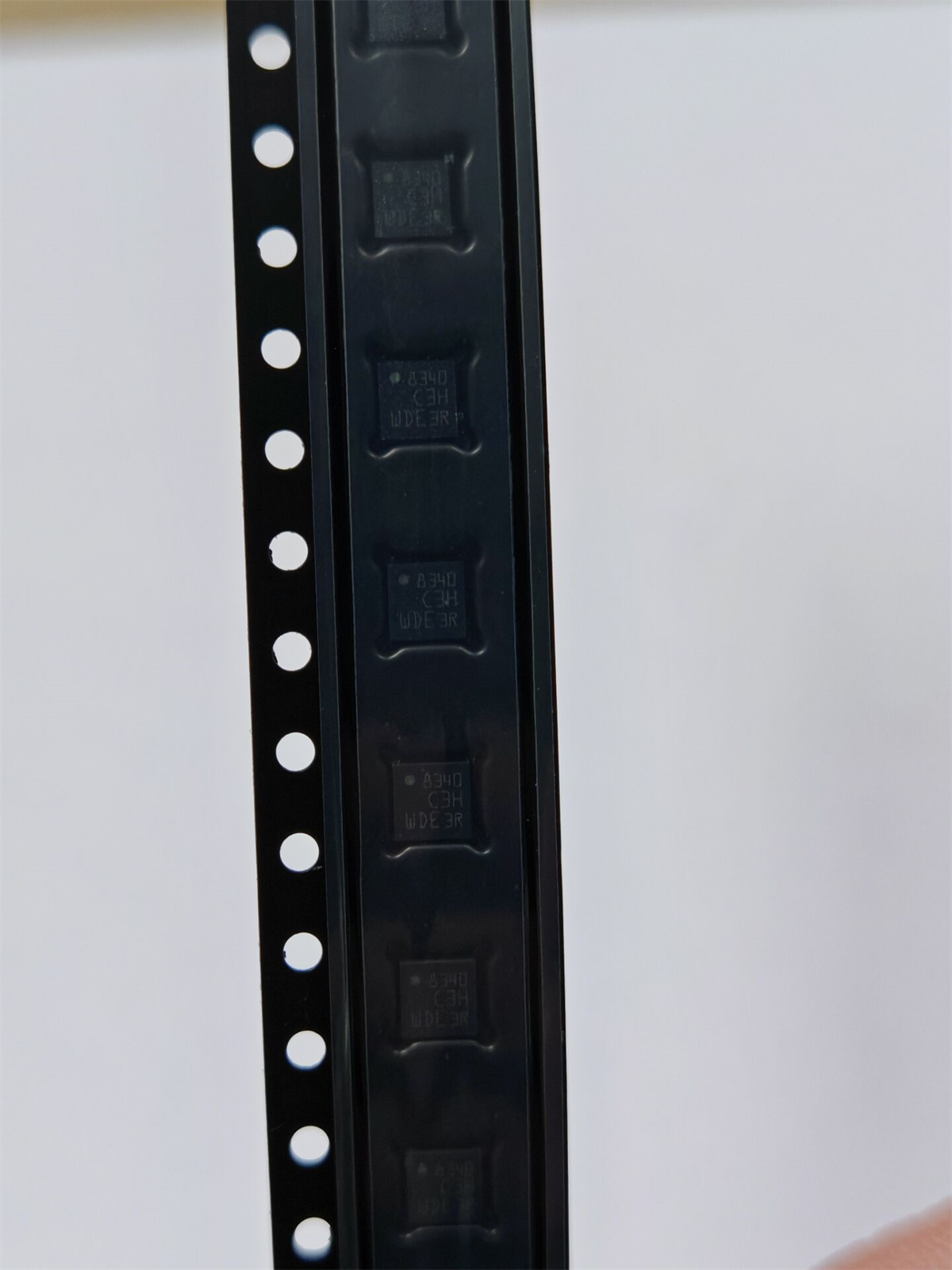

INA229AIDGSR
Brand: Texas Instruments
Texas Instruments INA229AIDGSR is a power management component designed for AI Servers & Low-Altitude Economy (Drone and UAV) and related applications. In stock at Superb Automation — request a quote for competitive pricing and fast delivery.
Product Specifications
INA229AIDGSR
Texas Instruments — Power Management & Signal Chain
Product Overview
The INA229AIDGSR from Texas Instruments is a power management / signal chain IC delivering high efficiency, precision regulation, and robust protection. Texas Instruments (TI) is a global leader in analog ICs, power management solutions, and embedded processors.
Superb Automation partners with leading brands including Qorvo, TI, ADI, XILINX, NVIDIA, Intel, ST, MACOM, Renesas, and Coilcraft to provide complete BOM and supply-chain solutions.
Key Features
- High-efficiency power conversion with low quiescent current
- Wide input voltage range with precision output regulation
- Integrated over-current, over-temperature, and short-circuit protection
- Small footprint packaging for space-constrained designs
- AEC-Q100 qualified options available for automotive applications
- Flexible sequencing and soft-start control
Key Specifications
| Input Voltage | V |
| Output Voltage | V |
| Output Current | A |
| Switching Frequency | kHz |
| Efficiency | % |
| Quiescent Current | µA |
| Topology | — |
| Package | — |
| Operating Temp | °C |
| Protection | — |
Applications
Industrial Automation
Automotive Electronics
Telecom Infrastructure
Server & Data Center Power
Medical Devices
Consumer Electronics
Request Quote — In Stock, 100% New & Original, Full Warranty
INA229AIDGSR: 85 V power monitor with a 20 bit converter and an SPI interface
INA229AIDGSR is a power, energy and charge monitor in the ten pin VSSOP body that measures across a shunt anywhere from 0.3 V below ground to 85 V, converts with a 20 bit stage at 1 uV of maximum offset, and reports over a four wire SPI port in a VSSOP body of 10 pins. The INA229 carries the same measurement chain as the INA228 and replaces the I2C port with SPI. Current, bus voltage, power, energy, charge and die temperature all come from one 20 bit converter, the shunt input has a plus or minus 163.84 mV range and a plus or minus 40.96 mV range, and the supply is 2.7 V to 5.5 V. Logic thresholds of 1.2 V make the port usable from 1.8 V controllers, and an alert output reports a threshold crossing without waiting for a poll.
Order code and package
| Order code | INA229AIDGSR |
| Function | power, energy, charge and temperature monitor |
| Common mode input range | minus 0.3 V to 85 V |
| Bus voltage input range | 0 V to 85 V |
| Shunt input range | plus or minus 163.84 mV or plus or minus 40.96 mV |
| Resolution | 20 bit delta sigma converter |
| Supply voltage | 2.7 V to 5.5 V |
| Interface | SPI with an alert output |
| Package | ten pin VSSOP, DGS body |
| Document | INA229 data sheet, SBOSA25 class |
Electrical parameters that decide the application
| Shunt offset voltage | plus or minus 0.3 uV typical, plus or minus 1 uV maximum |
| Offset drift | plus or minus 0.01 uV per C maximum |
| Gain error | plus or minus 0.05 percent maximum |
| Gain error drift | plus or minus 20 ppm per C maximum |
| Common mode rejection | 154 dB minimum, 170 dB typical |
| Power accuracy over the temperature range | 0.5 percent of full scale maximum |
| Energy and charge accuracy | 1.0 percent of full scale maximum |
| Alert response time | 75 us |
| Temperature sensor accuracy at 25 C | plus or minus 0.15 C typical, plus or minus 1 C maximum |
| Temperature sensor accuracy over the range | plus or minus 0.2 C typical, plus or minus 2 C maximum |
| Supply current | 640 uA typical, 750 uA maximum, 1.1 mA over the range |
| Shutdown current | 2.8 uA typical, 5 uA maximum |
| Power up time | 300 us |
| Logic input high threshold | 1.2 V |
| Operating temperature range | minus 40 C to 125 C |
Points to check before this part goes on a BOM
The measurement chain is the same one used in the I2C member of the family, down to the offset, drift and rejection figures, so the choice between them is a bus decision and not an accuracy decision. That is worth saying plainly because the two part numbers look like different products and behave as one silicon core behind two interfaces. A board that moves from I2C to SPI for bus reasons keeps its shunt, its voltage divider and its accuracy budget.
One microvolt of maximum offset across a 1 milliohm shunt is 1 mA, and the 40.96 mV range holds a 20 A load with 20 mV of signal. That leaves a factor of two of headroom for an overload before the range is exceeded, which is the margin a hot plug transient needs. The larger 163.84 mV range is there for a 10 milliohm shunt or for a load that can reach four times its nominal current, and the range is a register setting rather than a pin.
SPI is the reason to specify this version on a board with several monitors. Four monitors on one I2C bus need four addresses and a bus that can be held low by any one of them; four monitors on SPI need four chip selects and nothing else, so a stuck device cannot take the bus down. The cost is four pins on the controller instead of two, which on a 48 pin part is usually available and on a small controller sometimes is not.
The energy and charge registers accumulate in hardware, and that changes the error model. A firmware accumulator inherits the sampling jitter and any missed sample becomes a permanent offset in the total; a hardware accumulator integrates the converter output at a fixed rate and reports the sum. The residual error is then the offset drift of 0.01 uV per C, which over 40 C is 0.4 uV and across a 1 milliohm shunt is 0.4 mA. Over a thousand hours that is still 400 mAh, so the drift term does not disappear, it just stops being dominated by the sampling.
The 154 dB common mode rejection is what makes an 85 V part usable on a 60 V bus. A 60 V step attenuated by 154 dB is 0.38 uV at the input, which is below the 1 uV offset, so the common mode stops being the limiting term. That statement only holds if the shunt is a four wire connection with the sense lines taken from inside the pads: a two wire connection puts the trace resistance in series with the shunt and the rejection figure no longer describes the measurement.
Supply current of 640 uA typical and 1.1 mA at temperature is a system monitor budget, not a battery one: 1.1 mA is 26 mAh a day. The shutdown current of 2.8 uA and the 300 us power up time allow duty cycled operation, and a reading every ten seconds lands at an average of a few microamps. The alert output is what makes that practical, because a threshold crossing can wake the controller without the monitor having to be read continuously.
The die temperature channel reads the monitor and not the board, so it is useful for compensating the shunt and for a thermal alarm on the monitor itself. The 75 us alert response is the number that matters for fast events, and it is a signal rather than a trip: the pin announces that a limit was crossed and the controller decides what to do. A product that treats the alert as a protection trip has to define the latch and clear behaviour, otherwise the first event looks like a fault that never repeats.
Where this order code fits
This order code belongs on boards where the monitor shares an SPI bus with converters, memory or an FPGA and where an I2C bus would mean a second controller or a bridge. It fits 48 V and 60 V telecom rails, battery pack monitors, solar string combiners and server power shelves, and it is the part chosen when the energy or charge total has to be accumulated in hardware because the host cannot guarantee a fixed sample rate. Teams comparing it with a neighbouring part start from our Power Management Cross Reference page, and teams replacing a part that has gone end of life start from the OEM Procurement page.
Questions buyers ask
Is this part a drop in replacement for the I2C version? The pins carry the same measurement functions but the digital side is a different protocol, so the bus pins are not interchangeable and the firmware is not either. The package is the same ten pin VSSOP, so a board can be laid out for both, and the analogue side, the shunt and the voltage divider are identical. Moving between them is a bus change with a firmware change, not a component swap.
What shunt value suits a 48 V, 10 A rail? A 2 milliohm shunt gives 20 mV at 10 A, which sits in the 40.96 mV range with headroom to 20 A, and dissipates 0.2 W at full load. A 1 milliohm shunt halves the loss and halves the signal, which doubles the effect of the 1 uV offset. For a rail where the 10 A is continuous and the loss matters, the 1 milliohm part with the smaller range is the better trade.
Can the accumulators be read without disturbing the measurement? The energy and charge registers are 40 bit values and are read as several bytes, so a read that crosses an update can return a mixed value. The data sheet defines the read order and the latch behaviour for this reason. A controller that reads the high word, then the low word, and ignores the documented sequence will occasionally see a step that looks like a lost sample.
How fast does the monitor respond to an overcurrent? The alert responds in 75 us, which is much faster than a conversion at the slower settings and is the reason the pin exists. It is not a protection device: the threshold and the polarity are register settings, and the response to the alert belongs to the controller. For a real protection path the alert is a warning and a comparator or an efuse does the switching.
SUPERB holds and sources this line for production and repair demand, quoted against the exact ordering string with date codes, packing and country of origin stated on the offer. When a part is moving, the Component Lead Time Solutions page sets out the checks that keep a substitute from failing on the bench.