


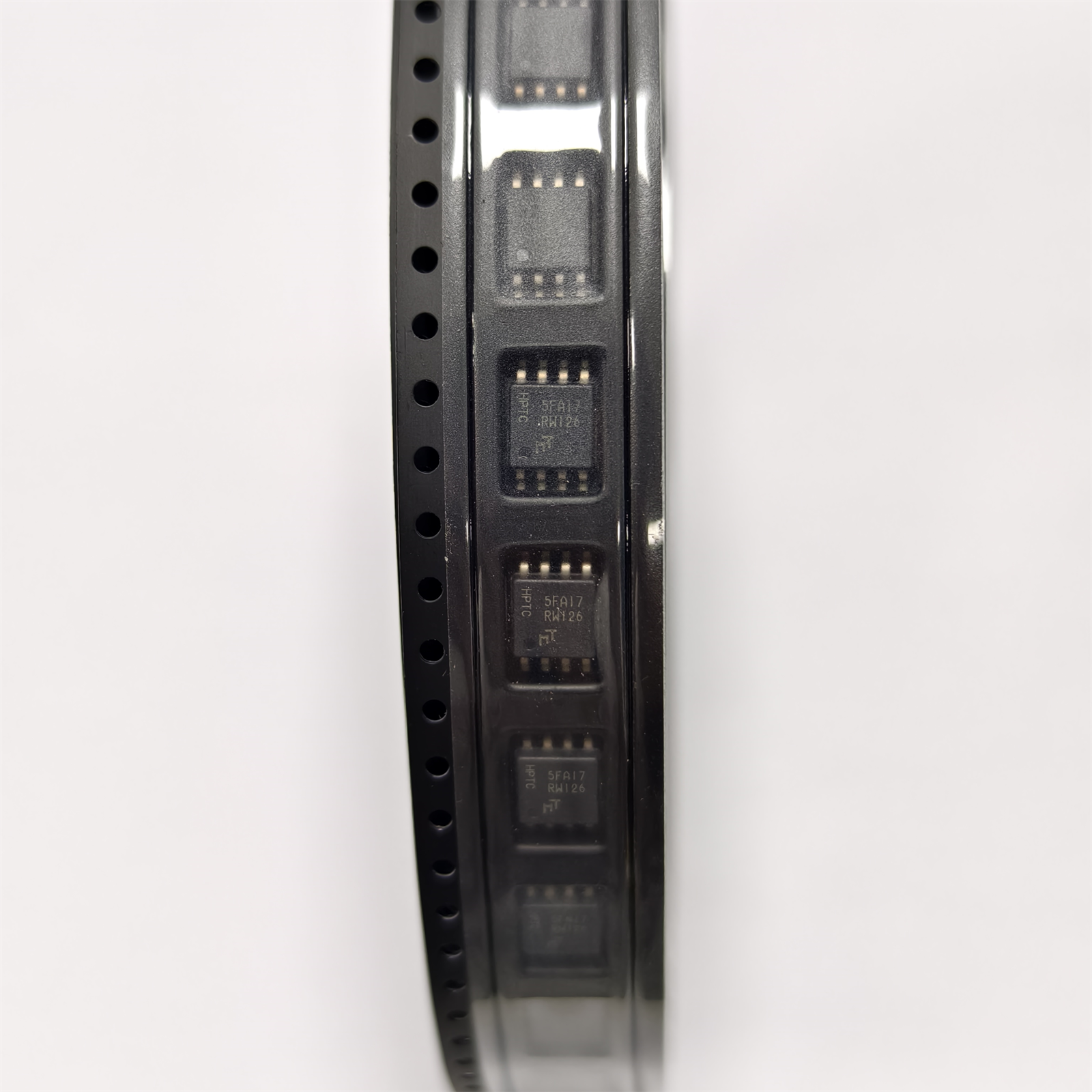

AT45DB041E-SSHN2B-T
Brand: Renesas / Dialog
The AT45DB041E-SSHN2B-T is Adesto's 4Mbit DataFlash serial NOR Flash, built on a proprietary dual SRAM buffer architecture that makes it the most efficient memory for data logging and event recording. Unlike standard NOR Flash, DataFlash lets the host program one SRAM buffer while simultaneously reading or erasing from the other — enabling continuous, gap-free data capture at 85MHz SPI clock. With 2048 pages x 256 bytes organization, 1.65V to 3.6V wide supply, and an 8-SOIC narrow package, it is ideal for IoT data loggers, industrial event recording, metering, and code shadowing applications where uninterrupted data streaming is essential.
Request Quo
Product Specifications
AT45DB041E-SSHN2B-T - Adesto 4Mbit DataFlash SPI NOR Flash, 85MHz, 8-SOIC
Adesto Technologies (Renesas) - Dual SRAM Buffer Architecture, 1.65-3.6V, Data Logging Optimized
MFR Part #: AT45DB041E-SSHN2B-TSuperb SKU: SUP-AT45DB041E-SSHN2B-T
In Stock - Ready to Ship
The AT45DB041E-SSHN2B-T is Adesto's 4Mbit DataFlash serial NOR Flash, built on a proprietary dual SRAM buffer architecture that makes it the most efficient memory for data logging and event recording. Unlike standard NOR Flash, DataFlash lets the host program one SRAM buffer while simultaneously reading or erasing from the other — enabling continuous, gap-free data capture at 85MHz SPI clock. With 2048 pages x 256 bytes organization, 1.65V to 3.6V wide supply, and an 8-SOIC narrow package, it is ideal for IoT data loggers, industrial event recording, metering, and code shadowing applications where uninterrupted data streaming is essential.
Request QuoteContact Sales
Key Features
4Mbit DataFlash density — 2048 pages x 256 bytes plus 128 Kbits of additional storage
Dual SRAM buffer architecture — program one buffer while reading/erasing the other, enabling continuous gap-free data logging
85MHz SPI interface — high-speed serial access for fast data transfer and code shadowing
Single/Dual SPI modes — flexible interface options for varying throughput requirements
1.65V to 3.6V supply voltage — wide voltage range compatible with 1.8V, 2.5V, and 3.3V systems
Page-oriented architecture — efficient page-level program and erase aligned with the dual-buffer design
8-SOIC narrow body package — compact footprint (SSHN suffix), compatible with standard SMD assembly
-40°C to +85°C operating range — industrial-grade reliability for field-deployed data logging
RoHS compliant — lead-free, meets international environmental standards
Technical Specifications
| Manufacturer | Adesto Technologies (Renesas) |
| Part Number | AT45DB041E-SSHN2B-T |
| Memory Type | DataFlash Serial NOR Flash (SPI) |
| Density | 4 Mbit (with extra 128 Kbits) |
| Organization | 2048 pages x 256 bytes |
| Interface | SPI (Single / Dual SPI) |
| Max Clock Frequency | 85 MHz |
| Supply Voltage | 1.65 V to 3.6 V |
| SRAM Buffers | Dual (2 x independent buffers) |
| Operating Temperature | -40C to +85C |
| Package | 8-SOIC narrow body (SSHN) |
| Mounting | Surface Mount (SMD) |
| Packaging | Tape & Reel (T) |
| RoHS | Compliant |
Product Details
Dual SRAM Buffer — Continuous Data Logging
The defining feature of DataFlash is its dual SRAM buffer architecture. Two independent SRAM buffers allow the host MCU to write incoming data into one buffer while the device simultaneously programs or erases the other buffer's contents to the flash array.
Why it matters: Standard NOR Flash introduces a programming "gap" — data capture must pause while a page is written to flash. DataFlash eliminates this gap via ping-pong buffering: fill Buffer 1, program Buffer 2, swap, repeat. This delivers uninterrupted, lossless data capture for mission-critical logging applications.
Additional benefit: The SRAM buffers also act as a read cache, allowing the host to read previously-buffered data at full SPI speed while a flash program operation is in progress.
Key Applications
IoT Data Logging — sensor data streams, environmental monitoring, continuous telemetry
Industrial Event Recording — PLC event logs, machine fault recording, production tracking
Smart Metering — energy/water meter consumption data logging
Code Shadowing — load firmware to SRAM for faster execution
Black Box / Flight Recorder — continuous data capture for post-incident analysis
Wearables & Medical — activity tracking, patient monitoring data buffers
Why Source AT45DB041E-SSHN2B-T from Superb Automation?
Embedded Memory BOM — DataFlash + MCU + sensors + passives, one consolidated PO
Pre-Programmed Options — Flash firmware or configuration data before assembly
SMT Assembly — 8-SOIC placement with automated optical inspection
Data Logger Design — SPI bus layout, buffer management, and power-loss data integrity guidance
25 Years Trusted — Electronic components + PCBA partner since 2000
Genuine Parts — Direct from authorized Renesas/Adesto channels, full lot traceability
Frequently Asked Questions
What is the AT45DB041E-SSHN2B-T used for?
A 4Mbit DataFlash serial NOR Flash for firmware storage, data logging, event recording, and code shadowing. Its dual SRAM buffer enables continuous gap-free data logging, making it ideal for IoT loggers, industrial event recording, and smart metering.
What is the difference between DataFlash and standard NOR Flash?
DataFlash uses a dual SRAM buffer architecture — the host can program one buffer while reading/erasing the other, enabling continuous data streaming. Standard NOR Flash has a single buffer and introduces a programming gap that interrupts data capture.
What is the page size and organization?
4Mbit organized as 2048 pages x 256 bytes, plus an additional 128 Kbits. The page-oriented architecture aligns with the dual-buffer design for efficient page-level programming at 85MHz SPI.
What voltage range does it support?
1.65V to 3.6V, compatible with 1.8V, 2.5V, and 3.3V systems. The wide range simplifies battery-powered and multi-voltage platform designs.
What is the "SSHN2B" suffix in the part number?
SSHN indicates the 8-SOIC narrow body package (150-mil width), and "2B" is the die/revision designation. The "T" suffix indicates tape & reel packaging. Other package options include WSON and UDFN for space-constrained designs.