

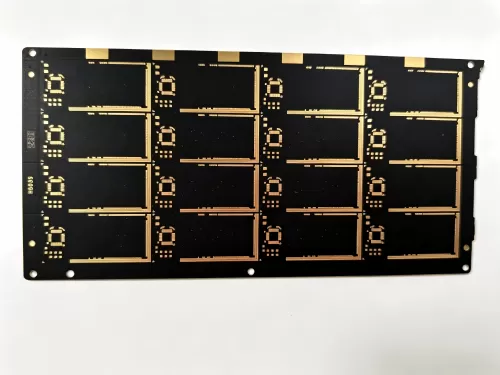
Multilayer BGA IC Package Substrate PCB Solution


Product Specifications
Product Overview
SUPERB provides advanced multilayer BGA IC package substrate PCB solutions for CPU packaging, power module processor packaging, and main control IC packaging applications.
Based on IC packaging-grade BT material, advanced die attach bonding processes, and multi-layer multi-step any-layer interconnection technology, SUPERB delivers ultra-thin BGA package substrates with excellent structural stability, high-density routing capability, and reliable semiconductor packaging performance.
With 0.3–0.4 mm ultra-thin substrate thickness, 0.03 mm ultra-fine line width and spacing, and precision micro via technology, our BGA IC package substrates are designed for high-performance semiconductor applications requiring high pin count, fine-pitch interconnection, and long-term reliability.
Key Specifications
| Item | Capability |
|---|---|
| Product Type | Multilayer BGA IC Package Substrate PCB |
| Applications | CPU Packaging, Power Module Processor Packaging, Main Control IC Packaging |
| Material | IC Packaging Grade BT Resin |
| Finished Board Thickness | 0.3 – 0.4 mm |
| Line Width / Spacing | 0.03 mm / 0.03 mm |
| Minimum Laser Hole | 0.05 mm |
| Via Technology | Laser Drilling + Copper Filling |
| Minimum Bonding Pad Size | 0.04 mm |
| Minimum BGA Pad Size | 0.05 mm |
| Interconnection Technology | Multi-layer, Multi-step Any-layer Interconnection |
| Solder Mask | AUS308 |
Product Applications
CPU IC Package Substrate
High-Performance CPU Core Packaging Solution
SUPERB multilayer BGA substrates support high-density CPU packaging requirements with ultra-fine 0.03 mm circuit routing technology.
Desktop CPU packaging
Server processor packaging
AI accelerator chip packaging
High pin-count BGA semiconductor packages
Power Module Processor Packaging
Thin BT Substrate for High-Power Applications
High-rigidity ultra-thin BT substrates provide excellent thermal stability and mechanical reliability for power semiconductor packaging.
New energy vehicle power modules
Industrial power management systems
DC-DC converter modules
High-current semiconductor devices
Main Control IC Packaging
Compact and Reliable IC Carrier Solution
Ultra-thin multilayer substrates provide stable signal transmission and high-density interconnection for advanced control chips.
Edge computing devices
Communication equipment
FPGA chip packaging
High-performance control systems
Automotive Semiconductor Modules
Reliable Packaging Substrate for Automotive Electronics
Using industrial-grade AUS308 solder mask technology, SUPERB BGA substrates provide enhanced chemical resistance, thermal reliability, and long-term operational stability.
Automotive semiconductor modules
Vehicle control systems
Intelligent automotive electronics
Industrial Electronic Chip Packaging
Long-Term Reliability for Industrial Applications
Robust BT-based BGA package substrates are designed for harsh industrial environments requiring stable performance and extended service life.
Industrial controllers
Servo drive systems
Power device packaging
Automation equipment
Product Features
Fine Pitch Multilayer BGA Substrate
SUPERB supports high-precision multilayer BGA IC substrate manufacturing with advanced build-up technology and ultra-thin structure capability.
Technical Advantages
Multi-layer, multi-step any-layer interconnection technology
0.03 mm ultra-fine line width and spacing
0.04 mm minimum bonding pad size
0.05 mm minimum BGA pad size
0.3–0.4 mm ultra-thin finished thickness
High-density routing capability for advanced BGA chips
IC Packaging Grade BT Material System
High-Performance BT Resin Substrate
SUPERB utilizes high-purity IC packaging-grade BT material to ensure excellent electrical, thermal, and mechanical performance.
Material Advantages
Ultra-low CTE matching silicon chip expansion characteristics
Excellent heat resistance during die bonding and reflow processes
Superior rigidity under ultra-thin substrate structures
Stable electrical performance for high-speed signal transmission
Compatible with semiconductor packaging requirements
Advanced Manufacturing Process
1. Laser Micro Via Drilling & Copper Filling
High-precision laser drilling technology creates 0.05 mm micro vias, combined with copper electroplating filling technology.
Improved electrical conductivity
Reduced via defects
Higher interconnection reliability
Better fine-pitch routing capability
2. Ultra-Fine Line Circuit Formation
Advanced circuit fabrication technology enables high-density routing within an ultra-thin substrate structure.
0.03 mm line width and spacing
High routing density
Precise etching control
Reliable signal transmission performance
3. Any-Layer Build-Up Interconnection Technology
Multi-step any-layer interconnection technology enables maximum routing flexibility for high pin-count BGA semiconductor devices.
Higher wiring density
Reduced substrate size
Improved package integration capability
Optimized electrical performance
4. Precision Bonding & BGA Pad Patterning
Strict dimensional and positional tolerance control ensures reliable die bonding and BGA assembly performance.
Stable die bonding process
High BGA assembly yield
Reliable semiconductor packaging performance
Consistent mass production quality
Technical Capabilities
SUPERB integrates semiconductor-grade manufacturing processes to provide reliable BGA IC package substrate solutions.
High-density multilayer BGA substrate fabrication
Ultra-thin BT substrate processing
Laser micro via formation
Copper-filled via technology
Fine-pitch circuit manufacturing
Precision bonding pad fabrication
Customized layer stack design
Prototype and mass production support
Why Choose SUPERB for BGA IC Package Substrate Solutions?
1. Full-Process BGA IC Package Substrate Manufacturing
Integrated solutions covering substrate design, fabrication, prototype validation, and mass production.
2. Experienced BT Material Processing Capability
Over 8 years of experience in precision BT substrate processing and ultra-thin PCB fabrication.
3. Customized Substrate Design Support
Flexible support for customized layer structures, routing requirements, BGA pitch, and package specifications.
4. Prototype to Mass Production Capability
Fast prototype delivery and stable high-volume production support for semiconductor packaging applications.
5. Semiconductor Supply Chain Integration
Supporting seamless connection with downstream IC packaging and assembly partners.
Request a Quote
Contact SUPERB for customized multilayer BGA IC package substrate PCB solutions.
Please provide the following information:
Substrate type
Material requirements
Layer count
BGA pitch
Package specification
Required quantity
Our engineering team will provide professional technical support and quotation based on your requirements.
Email: info@superb-tech.com
WhatsApp: +86 13396081443
Website: www.superb-tech.com