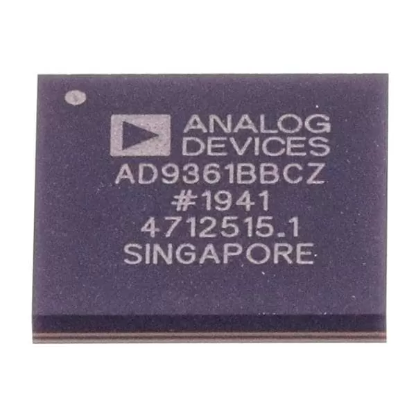
AD9361BBCZ
The AD9361BBCZ is a high-performance, highly integrated 2×2 RF Agile Transceiver™ from Analog Devices — the industry-standard RF front-end for software-defined radio (SDR), 4G base stations, drone datalinks, and wideband test & measurement systems. Covering 70 MHz to 6 GHz with tunable channel bandwidths from under 200 kHz to 56 MHz, it integrates dual independent receivers, dual transmitters, 12-bit ADCs/DACs, fractional-N frequency synthesizers, and configurable digital filters — all in a single 10 mm × 10 mm 144-ball CSP_BGA package.
Product Specifications
AD9361BBCZ — 70 MHz to 6 GHz RF Agile Transceiver™ by Analog Devices
The AD9361BBCZ is a high-performance, highly integrated 2×2 RF Agile Transceiver™ from Analog Devices — the industry-standard RF front-end for software-defined radio (SDR), 4G base stations, drone datalinks, and wideband test & measurement systems. Covering 70 MHz to 6 GHz with tunable channel bandwidths from under 200 kHz to 56 MHz, it integrates dual independent receivers, dual transmitters, 12-bit ADCs/DACs, fractional-N frequency synthesizers, and configurable digital filters — all in a single 10 mm × 10 mm 144-ball CSP_BGA package.
Quick Specifications
| Parameter | Value |
|---|---|
| Manufacturer | Analog Devices Inc. (ADI) |
| Part Number | AD9361BBCZ |
| Mouser # | 584-AD9361BBCZ |
| Product Family | AD9361 — RF Agile Transceiver™ |
| Configuration | 2 × Rx, 2 × Tx (2×2 MIMO Capable) |
| Frequency Range (Rx LO) | 70 MHz to 6,000 MHz |
| Frequency Range (Tx LO) | 47 MHz to 6,000 MHz |
| Tunable Channel Bandwidth | < 200 kHz to 56 MHz |
| Rx Inputs | 6 Differential or 12 Single-Ended |
| Tx Outputs | 4 Differential |
| ADC Resolution | 12-Bit, Σ-Δ, 640 MSPS (Max Sample Rate) |
| DAC Resolution | 12-Bit, 320 MSPS (Max Sample Rate) |
| Rx Noise Figure | < 2.5 dB (Typical, 800 MHz) |
| Rx Gain Range | 0 dB to 73 dB (MGC / AGC Modes) |
| Tx Output Power | Up to +8 dBm (Continuous Wave, 2.4 GHz) |
| Tx EVM | ≤ −40 dB (LTE 20 MHz, 64-QAM) |
| Frequency Synthesizers | Integrated Fractional-N PLLs for Rx, Tx, and BB |
| Duplex Modes | TDD (Time Division) and FDD (Frequency Division) |
| Digital Interface | LVDS or CMOS Parallel Data Port (12-bit I/Q) |
| SPI Control Interface | 4-Wire SPI for Register Configuration |
| Integrated Digital Filters | 128-Tap FIR + Programmable Decimation / Interpolation Chains |
| Rx Image Rejection | > 60 dB (After Calibration) |
| Supply Voltages | 1.3 V (Core/Analog), 1.8 V / 2.5 V / 3.3 V (Interface) |
| Power Consumption | ~1.1 W (1Rx/1Tx, 20 MHz BW, FDD Mode, Typical) |
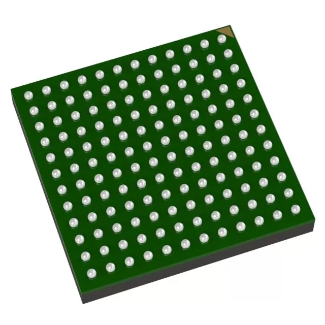
| Package | 144-Ball CSP_BGA (10 mm × 10 mm, 0.8 mm Pitch) |
| Operating Temperature | −40°C to +85°C (Industrial Range) |
| RoHS | Compliant |
| Evaluation Platforms | AD-FMCOMMS2/3/4/5, ADALM-PLUTO, USRP B2xx/E3xx |
| Supported Baseband Processors | Xilinx Zynq-7000, Altera Cyclone V / Arria 10, ADSP-BF70x |
| Linux Driver | Mainline IIO Subsystem Driver (Analog Devices / AD936x) |
| Reference Design | AD-FMCOMMS3-EBZ + Xilinx ZC706 / ZedBoard |
Product Overview
The AD9361 is a complete radio transceiver on a chip — what would have required 20+ discrete components a decade ago now fits inside a 10 mm × 10 mm BGA. Designed for 3G and 4G base station applications, the part has since become the foundational RF element across the entire software-defined radio ecosystem: from the $150 ADALM-PLUTO learning platform to multi-million-dollar electronic warfare systems.
At its core, the AD9361BBCZ integrates two independent direct-conversion receiver paths and two independent direct-conversion transmitter paths. Each path includes a low-noise amplifier (LNA), mixer, programmable gain amplifier (PGA), anti-alias filter, and a 12-bit Σ-Δ ADC on the receive side — and the inverse chain (DAC → filter → mixer → driver amplifier) on the transmit side. Two on-chip fractional-N phase-locked loops generate the receiver and transmitter local oscillator signals independently, enabling true FDD operation where Rx and Tx operate on different frequencies simultaneously.
The digital baseband interface is a configurable 12-bit parallel LVDS or CMOS port that maps directly to Xilinx Zynq, Altera SoC FPGAs, or ADI's own Blackfin DSPs. Combined with the mature, open-source AD936x Linux IIO driver, the AD9361 effectively becomes a "socket" for RF waveforms — define your modulation, bandwidth, and frequency in software, and the hardware follows.
Key Features & Benefits
Wideband Coverage: 70 MHz to 6 GHz in a Single Device
The AD9361's receiver LO tunes from 70 MHz to 6 GHz and the transmitter LO from 47 MHz to 6 GHz — covering essentially every band of commercial and military interest below 6 GHz in a single design. No band-specific front-end modules are required for:
Licensed cellular bands: LTE B1–B44, including TDD bands B38/B40/B41
ISM bands: 433 MHz, 868/915 MHz, 2.4 GHz, 5.8 GHz
GNSS L-band: GPS L1/L2, GLONASS, Galileo, BeiDou
Defense bands: L-band (1–2 GHz), S-band (2–4 GHz), C-band (4–6 GHz)
Unlicensed backhaul: 3.5 GHz CBRS, 5 GHz UNII
Drone / UAV datalinks: Custom waveforms from 900 MHz to 5.8 GHz
Programmable Bandwidth from <200 kHz to 56 MHz
Channel bandwidth is software-configurable via a chain of programmable decimation filters (Rx) and interpolation filters (Tx). This allows a single hardware design to support narrowband IoT signals (200 kHz NB-IoT) through wideband LTE carriers (20 MHz) and even custom wideband waveforms (56 MHz for spectrum monitoring). The 128-tap FIR filter provides additional channel selectivity and spectral shaping at the digital domain boundary.
Complete Receive Chain with Automatic Gain Control
Each receiver path delivers a total gain range of 0 to 73 dB in 1 dB steps, distributed across the LNA, mixer, transimpedance amplifier (TIA), and low-pass filter (LPF) stages. Three AGC modes are available:
Manual Gain Control (MGC) — Host processor sets gain levels directly via SPI. Best for deterministic test applications.
Fast Attack AGC — On-chip peak detectors adjust gain autonomously with sub-µs attack time. Essential for TDD systems with short Rx windows (Wi-Fi, LTE-TDD).
Slow Attack AGC — Averaging-based gain control for steady-signal environments (broadcast, spectrum monitoring).
The receiver achieves a noise figure below 2.5 dB at 800 MHz and maintains >60 dB image rejection after on-chip quadrature calibration — performance that previously required discrete, temperature-compensated RF front-ends.
High-Linearity Transmitter with Digital Predistortion-Ready Output
Each transmitter path delivers up to +8 dBm continuous wave output at 2.4 GHz with an error vector magnitude (EVM) of ≤ −40 dB for a 20 MHz LTE 64-QAM signal — comfortably meeting 3GPP TS 36.104 requirements for base station transmitters. The wide modulation bandwidth (56 MHz) supports advanced waveforms including OFDM, SC-FDMA, and direct-sequence spread spectrum. The transmitter output stage is designed to drive an external power amplifier (PA) directly, with sufficient linearity to allow digital predistortion (DPD) in the baseband processor.
Integrated Frequency Synthesizers — No External VCOs Required
Three independent fractional-N PLLs generate the Rx LO, Tx LO, and baseband sample clocks — all from a single external reference (typically 10–80 MHz). The fractional-N architecture provides <1 Hz frequency resolution, enabling fine Doppler compensation in satellite and radar applications. LO step time is under 250 µs, supporting fast frequency hopping in electronic warfare and spectrum monitoring use cases.
Mature Software Ecosystem — Not Just a Datasheet Part
What truly separates the AD9361 from competing wideband transceivers is the depth of its software support:
Mainline Linux Driver: The AD936x IIO (Industrial I/O) driver is upstream in the Linux kernel and actively maintained by Analog Devices. It provides full register-level control through sysfs and libiio APIs — no proprietary SDK required.
GNU Radio Integration: gr-iio out-of-tree module and official FMCOMMS blocks enable drag-and-drop SDR development in GNU Radio Companion.
MATLAB & Simulink: ADI provides the AD9361 Transceiver Toolbox and hardware support packages for direct MATLAB-to-hardware streaming and rapid prototyping.
Reference HDL: Open-source FPGA reference designs (Verilog/VHDL) for Xilinx Zynq-7000 and Altera SoC platforms, including DMA engines, JESD204B bridge logic (for AD9371/ADRV9009 migration), and IIO interface cores.
Python / C / C++ Bindings: libiio provides native bindings for Python, C, C++, and C# — stream I/Q samples and reconfigure the part from any language in <20 lines of code.
AD9361 Family — Choosing the Right Transceiver
| Feature | AD9361BBCZ | AD9363BBCZ | AD9364BBCZ | AD9371BBCZ |
|---|---|---|---|---|
| Channels | 2 Rx, 2 Tx | 2 Rx, 2 Tx | 1 Rx, 1 Tx | 2 Rx, 2 Tx, 2 ORx, 3 SnRx |
| Frequency Range | 70 MHz – 6 GHz | 70 MHz – 6 GHz | 70 MHz – 6 GHz | 300 MHz – 6 GHz |
| Max Bandwidth | 56 MHz | 20 MHz | 56 MHz | 100 MHz |
| Power (1Rx, 1Tx, 20 MHz) | ~1.1 W | ~0.9 W | ~1.1 W | ~3.5 W |
| DPD / CFR | Off-Chip (via FPGA) | Off-Chip | Off-Chip | On-Chip DPD Actuator |
| Observation Receiver | — | — | — | 2× Sniffer Rx + 3× ORx |
| Package | 144-CSP_BGA (10×10 mm) | 144-CSP_BGA (10×10 mm) | 144-CSP_BGA (10×10 mm) | 196-CSP_BGA (12×12 mm) |
| Digital Interface | LVDS / CMOS Parallel | LVDS / CMOS Parallel | LVDS / CMOS Parallel | JESD204B (4 Lanes) |
| Target Application | General-purpose 2×2 SDR | Cost-reduced 2×2 (BW-limited) | 1×1 SDR, Datalinks | 4G/5G Small Cells with DPD |
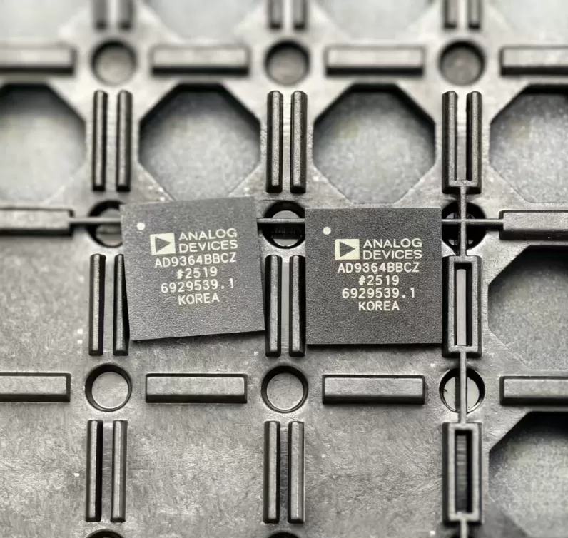
Selection guide: The AD9361 is the general-purpose flagship — pick it unless you have a specific reason to choose otherwise. The AD9363 is pin-compatible but firmware-limited to 20 MHz bandwidth (suitable for IoT gateways at lower cost). The AD9364 offers the same 56 MHz bandwidth as the AD9361 but in a single-channel configuration (drone datalinks, portable SDR). The AD9371 adds JESD204B, DPD, and observation receivers for 4G/5G small cells — at roughly 3× the power and cost.
Target Applications
Software-Defined Radio (SDR) Platforms
The AD9361 powers the world's most popular open SDR platforms: ADALM-PLUTO (ADI's $150 learning module), USRP B200mini/B205mini/B210/E310/E312/E313 (Ettus Research / NI), and the AD-FMCOMMS2/3/4/5 FMC mezzanine cards. Combined with GNU Radio, the AD9361 gives developers a full 70 MHz–6 GHz, 56 MHz bandwidth radio that can be repurposed from LTE base station to weather satellite receiver with a software change.
4G / 5G Small Cells & Base Stations
The AD9361 was originally designed for 3GPP-compliant base stations. Its EVM performance meets LTE 20 MHz 64-QAM requirements, and the integrated TDD/FDD support handles both duplex modes without external switches on the LO path. For 5G NR sub-6 GHz, the AD9361 serves in non-MIMO (SISO) small cells and repeaters where its 56 MHz bandwidth covers NR carrier configurations up to 50 MHz.
Drone / UAV Command & Telemetry Datalinks
The combination of sub-200 kHz narrowband modes (for long-range telemetry) and wideband 56 MHz modes (for HD video downlink) makes the AD9361 uniquely suited to multi-role UAV radios. Frequency agility across 900 MHz, 2.4 GHz, and 5.8 GHz enables dynamic spectrum access — critical in contested RF environments.
Test & Measurement / Spectrum Analysis
When paired with a Zynq SoC and open-source spectrum analysis firmware (e.g., PYNQ-SDR, Maia SDR), the AD9361 becomes a portable 70 MHz–6 GHz vector signal analyzer and generator. The 12-bit ADCs provide ~66 dB of instantaneous dynamic range, and the programmable FIR filter enables custom FFT binning for real-time spectral monitoring.
Electronic Warfare & SIGINT
Fast LO settling (<250 µs), wide instantaneous bandwidth (56 MHz), and full frequency coverage below 6 GHz make the AD9361 a popular choice for tactical signals intelligence (SIGINT) receivers and electronic attack (EA) exciters. The dual independent Rx paths enable direction-finding (DF) via phase-coherent reception on two antennas.
Satellite Communications Ground Terminals
From L-band Inmarsat terminals to S-band TT&C links and C-band VSAT modems, the AD9361 provides a single-chip modem front-end for satellite earth stations. The fractional-N synthesizer's <1 Hz resolution supports precision Doppler pre-compensation for LEO satellite tracking.
Evaluation & Development Ecosystem
The AD9361 is supported by one of the richest hardware evaluation ecosystems in the RF industry:
| Platform | Baseband Processor | Channels | Tunable Range | Typical Use Case |
|---|---|---|---|---|
| ADALM-PLUTO (ADALM-PLUTO) | Xilinx Zynq-7010 | 1 Rx, 1 Tx | 325 MHz – 3.8 GHz | Learning, prototyping, portable SDR |
| AD-FMCOMMS2-EBZ | External (FMC Connector) | 1 Rx, 1 Tx | 2.4 – 2.5 GHz (Tuned) | Wi-Fi / ISM band development |
| AD-FMCOMMS3-EBZ | External (FMC Connector) | 2 Rx, 2 Tx | 70 MHz – 6 GHz | Full-band SDR with ZC706/ZCU102 |
| AD-FMCOMMS4-EBZ | External (FMC Connector) | 1 Rx, 1 Tx | 70 MHz – 6 GHz | Single-channel wideband SDR |
| AD-FMCOMMS5-EBZ | External (FMC Connector) | 4 Rx, 4 Tx (2× AD9361) | 70 MHz – 6 GHz | 4×4 MIMO, beamforming, DF |
Frequently Asked Questions
What is the difference between AD9361BBCZ and AD9361BBCZ-REEL?
Identical silicon — the "-REEL" suffix indicates tape-and-reel packaging for automated assembly vs standard tray packaging (BBCZ without suffix). For prototype quantities (1–10 units), order the tray variant. For volume production, specify AD9361BBCZ-REEL.
How do I interface the AD9361 with an FPGA?
The AD9361 uses a parallel LVDS or CMOS data bus (12-bit I and 12-bit Q, plus DATA_CLK and FB_CLK for timing). This maps directly to Xilinx Zynq HP ports and Altera SoC FPGA I/O banks. ADI provides complete HDL reference designs with DMA, FIR filtering, and AXI-streaming interfaces. The AD9361 does NOT use JESD204B (that is the AD9371/ADRV9009 interface) — it uses a source-synchronous parallel interface that is simpler to implement on FPGAs without high-speed transceivers.
Can the AD9361 be used for 5G NR?
Yes — with caveats. The AD9361 supports 56 MHz instantaneous bandwidth, enough for 5G NR carriers up to 50 MHz (Δf = 30 kHz, 133 RB). It does not support carrier aggregation (CA) or massive MIMO (>2×2) natively — for those, consider the AD9375 or ADRV9009. For sub-6 GHz 5G small cells (SISO or 2×2 MIMO), the AD9361 is widely used and well understood.
How is the AD9361 different from the LimeSDR or HackRF?
The AD9361 provides significantly higher RF performance: noise figure <2.5 dB vs ~3.5 dB (LMS7002M), EVM ≤ −40 dB vs ~−30 dB, and on-chip AGC vs software-only gain control. The trade-off is cost and complexity — the AD9361 requires a capable baseband processor (Zynq-class FPGA) and careful PCB layout for the 144-ball BGA. The LimeSDR and HackRF are excellent for hobbyist SDR; the AD9361 is the choice for applications where link budget and modulation accuracy matter.
What is the minimum order quantity (MOQ) for AD9361BBCZ?
Contact SUPERB Automation for a tailored quote. We support prototype quantities (1–10 pieces) through full production volumes. Send your BOM to pcba@superb-tech.com — we quote within hours.
Is there a lead time issue with AD9361BBCZ?
The AD9361 is in active production at Analog Devices with stable multi-source wafer fabrication. SUPERB Automation works through trusted ADI distribution channels to secure competitive lead times. Contact us for current stock availability and volume pricing.
Can the AD9361 operate below 70 MHz?
The receiver LO minimum is specified at 70 MHz. For operation down to HF/VHF frequencies (1–70 MHz), designers typically add an external upconverter/downconverter stage or select the ADRV9002/ADRV9003 which has a native 30 MHz lower limit. The AD9361's digital interface and baseband processing chain can handle arbitrarily low IF frequencies when paired with external mixing.
Ordering Information
| Orderable Part Number | Package | Packaging | Temperature Range |
|---|---|---|---|
| AD9361BBCZ | 144-Ball CSP_BGA (10×10 mm) | Tray | −40°C to +85°C |
| AD9361BBCZ-REEL | 144-Ball CSP_BGA (10×10 mm) | Tape & Reel | −40°C to +85°C |
Design Resources
Datasheet: AD9361 Data Sheet (Rev F or later) — 36 pages
Reference Manual: AD9361 Reference Manual UG-570 — ~280 pages covering register map, filter configuration, gain tables, state machine transitions, and calibration procedures
Linux Driver: AD936x IIO driver — mainline Linux kernel (drivers/iio/adc/ad9361.c) + libiio userspace library
FPGA HDL: ADI HDL reference designs on GitHub (analogdevicesinc/hdl) — targeting Zynq-7000, Zynq UltraScale+, Altera Cyclone V / Arria 10
MATLAB Support: AD936x Filter Wizard + AD9361 Transceiver Toolbox for streaming and hardware-in-the-loop
GNU Radio: gr-iio OOT module + FMCOMMS source/sink blocks for graphical SDR development
IBIS Model: Available for SI simulation of the LVDS/CMOS digital interface
Footprint / Symbol: Available from SnapEDA, Ultra Librarian for Altium, Eagle, KiCad, OrCAD
Request a Quote
SUPERB Automation supplies genuine Analog Devices AD9361BBCZ RF Agile Transceivers with full traceability and competitive lead times. From prototype quantities on the AD-FMCOMMS3-EBZ eval platform to volume production for SDR and base station deployments, we deliver.
Send your BOM or inquiry to pcba@superb-tech.com — we quote within hours. For full system builds, include your FPGA baseband selection and RF front-end requirements for a complete BOM + PCBA assembly quote.
SUPERB Automation — We Make It Real. Since 2000.