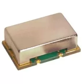
UCC28C41QDRQ1
Brand: Texas Instruments
Texas Instruments UCC28C41QDRQ1 is a power management component designed for AI Servers & Low-Altitude Economy (Drone and UAV) and related applications. In stock at Superb Automation — request a quote for competitive pricing and fast delivery.
Product Specifications
UCC28C41QDRQ1
Texas Instruments — Power Management & Signal Chain
Product Overview
The UCC28C41QDRQ1 from Texas Instruments is a power management / signal chain IC delivering high efficiency, precision regulation, and robust protection. Texas Instruments (TI) is a global leader in analog ICs, power management solutions, and embedded processors.
Superb Automation partners with leading brands including Qorvo, TI, ADI, XILINX, NVIDIA, Intel, ST, MACOM, Renesas, and Coilcraft to provide complete BOM and supply-chain solutions.
Key Features
- High-efficiency power conversion with low quiescent current
- Wide input voltage range with precision output regulation
- Integrated over-current, over-temperature, and short-circuit protection
- Small footprint packaging for space-constrained designs
- AEC-Q100 qualified options available for automotive applications
- Flexible sequencing and soft-start control
Key Specifications
| Input Voltage | V |
| Output Voltage | V |
| Output Current | A |
| Switching Frequency | kHz |
| Efficiency | % |
| Quiescent Current | µA |
| Topology | — |
| Package | — |
| Operating Temp | °C |
| Protection | — |
Applications
Industrial Automation
Automotive Electronics
Telecom Infrastructure
Server & Data Center Power
Medical Devices
Consumer Electronics
Request Quote — In Stock, 100% New & Original, Full Warranty
UCC28C41QDRQ1: an automotive current mode PWM controller with a 5 V reference trimmed to 1 per cent, a 1 MHz oscillator ceiling, 35 ns of current sense to output delay and a 50 per cent maximum duty cycle, in the eight pin SOIC on a 2500 piece reel
UCC28C41QDRQ1 is a fixed frequency peak current mode controller that drives a power FET gate directly, with an undervoltage lockout chosen for a battery rail and a toggle flip-flop that halves the output frequency and caps the duty cycle in a SOIC body of 8 pins. The D body is 4.90 mm by 3.91 mm, and the Q1 suffix carries the automotive qualification with an AEC-Q100 grade 1 temperature range rather than a separate die.
Order code and package
| Catalogue string | UCC28C41QDRQ1, where 41 is the 50 per cent duty member, Q is the automotive qualifier, D is the eight pin SOIC, R is the large reel and the closing Q1 repeats the qualification |
| Body | SOIC, D, eight pins, 4.90 mm by 3.91 mm, the same outline the industrial UCC28C4x family uses |
| Reel | 2500 pieces on a large tape and reel on the addendum dated 2022, with the .A revision row at the same quantity |
| Finish and moisture | NIPDAU plating, moisture level 1 at 260 C with no floor life limit |
| Qualification | AEC-Q100 grade 1, minus 40 to 125 C ambient, HBM classification level 2 at plus or minus 2 kV and CDM level C4B at 750 V |
| Marking | 28C41Q on the body, which is the only visible difference from the industrial part |
| Document | SLUSA12G, December 2009, revised November 2022 |
| Status | Active and in production, with all six members of the family listed on the same addendum |
| Functional safety | listed as functional safety capable, with documentation available to support a system level safety case |
Electrical parameters that decide the application
| Bias range | 15 V is the table condition, with an absolute maximum of 18 V and a start threshold of 7 V on this member |
| Lockout, rising | 6.5 V minimum, 7.0 V typical and 7.5 V maximum, which is the version for a 12 V battery rail that has to start below 9 V |
| Lockout, falling | 6.1 V minimum, 6.6 V typical and 7.1 V maximum, giving about 0.4 V of hysteresis |
| Start current | 50 uA typical and 100 uA maximum, so a resistor from the high voltage rail can charge the bias capacitor |
| Run current | 2.3 mA typical and 3 mA maximum with no gate load, which is small enough that a bias winding can feed it |
| Reference | 5 V initial accuracy of 1 per cent, 4.9 V to 5.1 V, with a total variation of 4.82 V to 5.18 V over temperature and 50 uV of noise from 10 Hz to 10 kHz |
| Reference current | 45 mA typical and 55 mA maximum into a short, so the reference can feed a divider and a timing resistor but not a load |
| Oscillator | 53 kHz with a 10 kOhm timing resistor and a 3.3 nF timing capacitor, 50.5 kHz to 55 kHz at 25 C, with 1 MHz as the family ceiling |
| Discharge current | 8.4 mA typical and 9.5 mA maximum at the timing pin, trimmed so the maximum duty cycle does not drift with temperature |
| Error amplifier | 2.5 V reference input with 1 per cent initial accuracy, 90 dB of open loop gain and 1.5 MHz of unity gain bandwidth |
| Current sense | 3 V per V of gain, 1.0 V maximum input signal, 1.15 V of COMP to CS offset and 35 ns typical, 70 ns maximum of delay from the sense pin to the output |
| Output stage | plus or minus 1 A peak, 25 ns rise and 20 ns fall into 1 nF, with 15 Ohm of pull-down and 25 Ohm of pull-up at 200 mA |
| Duty cycle | 50 per cent maximum on this member because the output runs at half the oscillator frequency, against 96 per cent on the UCC28C42-Q1 and UCC28C43-Q1 |
What the eight pins do
| COMP, pin 1 | the error amplifier output, brought out for the compensation network and used as the reference for the current loop |
| FB, pin 2 | the inverting input of the error amplifier, which takes the feedback divider and needs 2.5 V to sit in regulation |
| CS, pin 3 | the current sense input and the non-inverting input of the PWM comparator, where 1 V of signal ends the on time |
| RT/CT, pin 4 | the timing node, with a resistor to VREF and a capacitor to ground setting the oscillator frequency and the maximum duty cycle |
| GND, pin 5 | the return for the output driver and the control logic, and the point the current sense resistor returns to |
| OUT, pin 6 | the gate drive output, which is at half the oscillator frequency on this member and limited to 50 per cent duty |
| VDD, pin 7 | the bias input, with a 7 V start threshold and a 6.6 V stop threshold on this member |
| VREF, pin 8 | the 5 V reference output, which also feeds the timing resistor, so loading it changes the frequency |
Points to check before this part goes on a BOM
The toggle flip-flop is the reason to choose the 41 over the 42. On this member the output changes state on every oscillator cycle, so the switching frequency is half the oscillator frequency and the duty cycle cannot exceed 50 per cent. That is exactly what a single ended forward converter or a flyback running in continuous conduction needs, because the transformer core has to be reset in the off time and a duty cycle above 50 per cent leaves no room. The price is that the same transformer delivers about half the power it would with a 96 per cent duty member, and a board that needs the power either halves the primary inductance or moves to the UCC28C42-Q1.
The 7 V lockout is chosen for a battery rail and not for an off-line rail. A 12 V automotive rail sits at 13.8 V in normal operation and drops to 6 V during a cold crank, so a controller that starts at 14.5 V would restart the converter on every crank and a controller that starts at 7 V keeps it running until the rail is nearly gone. The same 7 V threshold is wrong for a 48 V telecom rail, where the converter should not start until the rail is at 36 V, and the family answers that with the 14.5 V members. The lockout is a property of the letter in the part number, and it is the first thing to check against the rail the board actually sees.
The current sense path has three numbers that are easy to mix up. The maximum input signal is 1.0 V, the gain from the sense pin to the comparator is 3 V per V, and the COMP to CS offset is 1.15 V, which sets the minimum on time at low load. A 35 ns delay from the sense pin to the output is fast for a controller of this age and still slow compared with the di/dt of a modern FET, so the leading edge spike has to be filtered with an RC network at the pin. That filter adds delay of its own, and a 1 kOhm and 100 pF pair adds 100 ns which shows up as a current limit that is higher than the nominal value at high line.
The 5 V reference is trimmed to 1 per cent at 25 C and specified to stay within 4.82 V and 5.18 V over the full range, which is nearly 4 per cent and is what a divider has to be calculated against. Loading the reference with the timing resistor, which is how the oscillator is fed, already draws about 0.5 mA, and adding a divider that draws 1 mA is inside the 20 mA the reference can deliver. What is not inside the rating is a reference used as a logic supply or a capacitor that leaks; the reference survives a short to ground at 55 mA but the regulation of everything else on the chip degrades while it does.
The automotive qualification is worth reading as a set of limits rather than a badge. Grade 1 means minus 40 to 125 C ambient, HBM level 2 is plus or minus 2 kV, and CDM level C4B is 750 V, which are the levels a module built on a production line will actually see. The functional safety listing means the vendor has documentation for a system level safety case, not that the part is certified for a safety function on its own. A board that needs a safety element out of context has to read that documentation and decide whether the failure modes it describes match the ones the system analysis found.
Power dissipation in the controller is small and dominated by the gate charge. Driving 20 nC at 12 V and 100 kHz is 24 mW, and the 2.3 mA of run current at 15 V is 35 mW, so the part dissipates well under 100 mW and the eight pin body stays cool. The number that matters is the peak output current during the switching transition, because 1 A into the gate for 25 ns is a current that flows through the bond wires and the ground pin, and a poor ground return turns that into a voltage spike on the CS pin. The current sense resistor has to return to the same point the GND pin uses, and that single connection is the difference between a stable current limit and one that trips early at high line.
Reading the letters in UCC28C41QDRQ1
The string decodes in four parts and every part is a choice. The 41 is the 50 per cent duty member with a 7 V lockout, the Q is the automotive qualifier, the D is the eight pin SOIC and the R is the large tape and reel, with the trailing Q1 repeating the automotive grade. The same family offers the 42 and 44 with a 14.5 V lockout and 96 per cent duty, the 43 and 45 with a 8.4 V lockout, and the 40 with a 7 V lockout and 96 per cent duty. Reading the four characters in the right order is the difference between a converter that starts on a crank and one that does not.
The industrial UCC28C4x parts share the die and the electrical table, and the automotive parts differ in qualification and marking rather than in function. A buyer who needs the automotive part cannot substitute the industrial one on a production order, even though the two are pin compatible and the electrical table is identical.
What a 50 per cent duty limit does to the transformer
A flyback running in continuous conduction with a 50 per cent limit transfers energy during half the period, so the primary current ramps from a minimum to a peak in that time and the transformer stores what the secondary takes during the other half. The same core with a 96 per cent duty member can store the same energy at a lower peak current, which means less copper loss and a smaller core for the same output. The 41 is chosen when the leakage inductance and the switch voltage demand a long reset time, not when the output power is the priority.
The practical effect is that a board built around the 41 with a 10 W output needs a primary inductance of about half the value a 42 would need at the same frequency, and the transformer therefore has a larger gap and more turns. At 20 W the difference becomes a core size, and that is the point at which the 42 with a 14.5 V lockout and a 96 per cent duty is the better part if the rail allows it.
Where this order code fits
Isolated bias supplies and DC to DC converters in electric vehicle on-board chargers and traction inverters, HVAC compressor supplies, and 12 V battery rails where the converter has to keep running through a cold crank Teams comparing it with a neighbouring part start from our Power Management Cross Reference page, and teams replacing a part that has gone end of life start from the Component Lead Time Solutions page.
Questions buyers ask
Why is the duty cycle limited to 50 per cent? The output runs at half the oscillator frequency through a toggle flip-flop, which guarantees the transformer has an equal reset interval.
Can it run from a 12 V rail? Yes. The start threshold is 7 V, so it starts on a rail that has dropped during a crank and keeps running down to 6.6 V.
How fast is the over-current response? 35 ns typical and 70 ns maximum from the current sense pin to the output, before the filter at the pin adds its own delay.
Does the reference feed the oscillator? Yes, through the timing resistor, which is why loading the 5 V reference with anything else changes the switching frequency.
Is the industrial part a substitute? Not on an automotive order. The die and the electrical table are shared, but the qualification and the marking are not.
SUPERB holds and sources this line for production and repair demand, quoted against the exact ordering string with date codes, packing and country of origin stated on the offer. When a part is moving, the How to Verify a Drop in Replacement page sets out the checks that keep a substitute from failing on the bench.