
TPS7A201825PDQNR
Brand: Texas Instruments
Texas Instruments TPS7A201825PDQNR is a power management component designed for AI Servers & Low-Altitude Economy (Drone and UAV) and related applications. In stock at Superb Automation — request a quote for competitive pricing and fast delivery.
Product Specifications
TPS7A201825PDQNR
Texas Instruments — Power Management & Signal Chain
Product Overview
The TPS7A201825PDQNR from Texas Instruments is a power management / signal chain IC delivering high efficiency, precision regulation, and robust protection. Texas Instruments (TI) is a global leader in analog ICs, power management solutions, and embedded processors.
Superb Automation partners with leading brands including Qorvo, TI, ADI, XILINX, NVIDIA, Intel, ST, MACOM, Renesas, and Coilcraft to provide complete BOM and supply-chain solutions.
Key Features
- High-efficiency power conversion with low quiescent current
- Wide input voltage range with precision output regulation
- Integrated over-current, over-temperature, and short-circuit protection
- Small footprint packaging for space-constrained designs
- AEC-Q100 qualified options available for automotive applications
- Flexible sequencing and soft-start control
Key Specifications
| Input Voltage | V |
| Output Voltage | V |
| Output Current | A |
| Switching Frequency | kHz |
| Efficiency | % |
| Quiescent Current | µA |
| Topology | — |
| Package | — |
| Operating Temp | °C |
| Protection | — |
Applications
Industrial Automation
Automotive Electronics
Telecom Infrastructure
Server & Data Center Power
Medical Devices
Consumer Electronics
Request Quote — In Stock, 100% New & Original, Full Warranty
TPS7A201825PDQNR: the 1.825 V trim of the low noise 300 mA regulator
The TPS7A201825PDQNR is a 1.825 V fixed output of the TPS7A20 family, a 300 mA regulator specified at 7 uV RMS of output noise and 95 dB of rejection at 1 kHz without a noise bypass capacitor. The trim value looks arbitrary until the data sheet is read closely: 1.825 V is the mid point the vendor uses when it characterises accuracy and noise across the family, because it sits inside the band where the pass element and the reference are both in their most representative operating points.
The part takes 1.6 V to 6.0 V at the input and covers 0.8 V to 5.5 V at the output, with a maximum tolerance of 1.5 percent over the full junction range. The quiescent current is 6.5 uA, which is high for a battery product and low for a low noise regulator, and that trade is the whole point of the family: it is built for RF and analog circuits that need a quiet rail and cannot afford a bypass capacitor on a crowded board.
Key electrical data for the 1.825 V point
| Input range | 1.6 V to 6.0 V, 2.025 V minimum for regulation at 300 mA |
| Output current | 300 mA, current limit 360 mA to 730 mA, short circuit 160 mA |
| Quiescent current | 6.5 uA typical at no load, 8.5 uA maximum in the four pin body |
| Accuracy | plus or minus 1.5 percent maximum over minus 40 to 125 C |
| Dropout at 300 mA | 690 mV in the 0.8 V to 1.0 V band, 140 mV at 3.3 V output |
| Rejection | 95 dB at 1 kHz into 20 mA, 75 dB at 10 kHz, 45 dB at 1 MHz |
| Noise | 7 uV RMS over 10 Hz to 100 kHz with no bypass capacitor fitted |
Package, marking and reel data
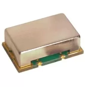
| Body | X2SON DQN, 4 pins, 1.0 mm by 1.0 mm |
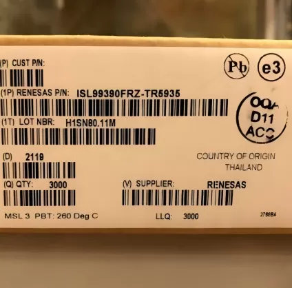
| Reel | 3000 pieces, large tape and reel, 180 mm carrier, 8 mm tape |
| Finish | NIPDAU, with a NIPDAUAG alternate row on the same code |
| Moisture | level 1, 260 C peak reflow, unlimited floor life |
| Marking | IQ |
Where a 1.825 V low noise rail belongs
The natural home is a radio or a sensor front end that runs at about 1.8 V and cannot tolerate the switching residue of the converter that feeds it. A phase locked loop, a voltage controlled oscillator, an analog to digital converter reference buffer or a low noise amplifier bias all fall into that group. Because the rail is only 1.825 V and the input can be 6 V, the regulator also works directly from a battery or a 3.3 V rail without a pre regulator, at the cost of dissipating the difference.
Two points decide whether the noise figure survives the board. The output capacitor has to be a ceramic of 1 uF or more placed within a couple of millimetres of the pin, and the ground return has to be a plane rather than a trace, because the rejection above 100 kHz depends on it. The enable pin has a smart pulldown, so leaving it floating keeps the rail off, which is the behaviour a bring up sequence usually wants.
Buyer questions on the 1.825 V code
Why 1.825 V rather than a round 1.8 V? It is a factory trim available in the family, and it is the value the vendor uses in its own accuracy and noise conditions. A product that needs exactly 1.8 V should order the 1.8 V code instead, which exists in the same bodies.
Does the part need a noise bypass capacitor? No, and that is the reason to choose it. The 7 uV RMS figure is achieved with a 1 uF output capacitor alone, so there is no extra pin, no extra component and no extra placement constraint.
What is the current limit window? 360 mA minimum, 520 mA typical and 730 mA maximum in the four pin body, with a 160 mA short circuit figure. A rail that has to survive an inrush above 300 mA should be checked against the minimum rather than the typical.
Sourcing a low noise regulator
Noise and rejection are the two parameters that a data sheet swap usually loses, so an alternative part has to be compared on the same conditions rather than on the headline. Component obsolescence management covers how we keep a qualified alternative on file for a rail like this, and supplier quality audit describes the checks behind a reel that is bought outside the franchised channel.
The rejection figures are the reason to pay for this part rather than a cheaper 300 mA regulator: 95 dB at 1 kHz into 20 mA, 75 dB at 10 kHz, 60 dB at 100 kHz and 45 dB at 1 MHz, all from a 1 uF ceramic output capacitor with no bypass pin. Above 100 kHz the loop has less control, so the board ground return does as much work as the silicon, and a rail that measures badly on the bench is usually a long return rather than a part outside its window. Quiescent current is 6.5 uA typical and 8.5 uA maximum in this body, which is the price of the noise floor.