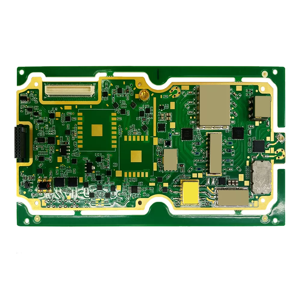
TPS73132DBVR
Brand: Texas Instruments
Texas Instruments TPS73132DBVR is a power management component designed for AI Servers & Low-Altitude Economy (Drone and UAV) and related applications. In stock at Superb Automation — request a quote for competitive pricing and fast delivery.
Product Specifications
TPS73132DBVR
Texas Instruments — Power Management & Signal Chain
Product Overview
The TPS73132DBVR from Texas Instruments is a power management / signal chain IC delivering high efficiency, precision regulation, and robust protection. Texas Instruments (TI) is a global leader in analog ICs, power management solutions, and embedded processors.
Superb Automation partners with leading brands including Qorvo, TI, ADI, XILINX, NVIDIA, Intel, ST, MACOM, Renesas, and Coilcraft to provide complete BOM and supply-chain solutions.
Key Features
- High-efficiency power conversion with low quiescent current
- Wide input voltage range with precision output regulation
- Integrated over-current, over-temperature, and short-circuit protection
- Small footprint packaging for space-constrained designs
- AEC-Q100 qualified options available for automotive applications
- Flexible sequencing and soft-start control
Key Specifications
| Input Voltage | V |
| Output Voltage | V |
| Output Current | A |
| Switching Frequency | kHz |
| Efficiency | % |
| Quiescent Current | µA |
| Topology | — |
| Package | — |
| Operating Temp | °C |
| Protection | — |
Applications
Industrial Automation
Automotive Electronics
Telecom Infrastructure
Server & Data Center Power
Medical Devices
Consumer Electronics
Request Quote — In Stock, 100% New & Original, Full Warranty
TPS73132DBVR 3.2 V regulator that needs no output capacitor
The TPS73132DBVR is the 3.2 V fixed member of the TPS731 family, a 150 mA regulator that runs from 1.7 V to 5.5 V and is specified as stable with no output capacitor at all. That is the whole point of the part. Every other regulator in this class asks for at least one microfarad of ceramic on the output, and on a board with a dozen small rails those capacitors take area, add a placement step and become the component most likely to be missing from a kit. The TPS731 removes that requirement, and the vendor document states it twice, once in the pin table and once in the description.
The silicon is an NMOS pass device in a follower configuration, so the pole that would normally need an output capacitor to compensate moves with the load instead. The cost is a ground current that runs at 400 microamp typical, which is high for a 150 mA part by modern standards, and a dropout that is only 30 mV typical because the follower needs less headroom than a common source pass device.
Key parameters from the SBVS034P document
| Input range | 1.7 V to 5.5 V, minimum also set by output plus dropout |
| Output | 3.2 V fixed, adjustable member uses a 1.204 V reference |
| Current | 150 mA continuous |
| Accuracy | 0.5 percent typical, 1 percent maximum over load, line and temperature |
| Dropout | 30 mV typical, 100 mV maximum at 150 mA |
| Output capacitor | None required for stability, 0.1 microfarad used for the published transient curves |
| Quiescent current | 400 microamp typical, 550 microamp maximum on the legacy chip and 580 on the current chip |
| Shutdown current | 0.02 microamp typical, 1 microamp maximum |
| Current limit | 150 mA minimum, 360 mA maximum at the 0.9 times nominal output point |
| Reverse leakage | 0.1 microamp typical, 10 microamp maximum with the enable held low |
| Rejection | 58 dB at 100 Hz at 150 mA, 37 dB at 10 kHz |
| Package | DBV five pin SOT-23, marking BYS, 3000 pieces on a large reel |
Why the 3.2 V point exists
A 3.2 V rail is not a standard logic voltage, and that is the reason a buyer sometimes cannot find a second source for it. It appears in products that stack a 3.3 V rail with a diode drop, in battery instruments that need the rail above the 3.0 V cut off of their cell chemistry, and in older telecom line cards. The adjustable member of this family covers the same point from a divider, and the fixed member removes two resistors and the tolerance they add to the output.
Where a board already carries 3.3 V and needs a slightly lower rail for a sensitive analog block, the fixed 3.2 V part is a cleaner answer than a series diode, because the diode drop moves with current and the regulator does not. The trade is that the 3.2 V rail then tracks the 3.3 V rail's accuracy, which is usually 2 percent, rather than being independently trimmed.
Where this part fits
Handheld instruments, portable medical monitors, sensor nodes and legacy telecom cards use this family when the rail has to survive a missing capacitor on the line. The family substitution data we keep for older boards is under obsolete RF part replacement, and the rules we apply before accepting a capacitor free substitute are in how to verify a drop in replacement.
What to check before a purchase order
Check the quiescent current against the standby budget. At 400 microamp this part is roughly twice the ground current of a 150 mA regulator with an output capacitor, and for a product that sleeps for weeks on a small cell that difference decides the battery life. The capacitor free feature is worth the current only where the capacitor itself is the problem, which is a common situation on a dense board and a rare one on a mains powered product.
Check the dropout against the real input. The 30 mV typical figure is quoted at 150 mA on the legacy silicon, and the fixed 3.2 V member needs at least 3.3 V at the input for the 100 mV maximum to hold over temperature. A rail derived from a silicon diode ORing two supplies will sit below that in the last part of a battery discharge, and the regulator then follows the input down instead of regulating.
Questions that come up on this part
Does the part oscillate with a large output capacitor? No. The document describes it as stable with any capacitor value or type, which is the unusual side of the NMOS follower topology. That makes it usable on a board that already carries bulk capacitance.
What happens when the output is held above the input? The reverse leakage row specifies 0.1 microamp typical and 10 microamp maximum with the enable low, so the output does not discharge back through the pass device when the upstream supply is switched off.