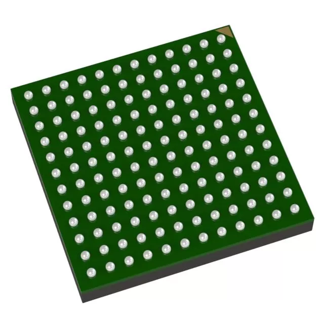
TPS2066DR
Brand: Texas Instruments
Texas Instruments TPS2066DR is a power management component designed for AI Servers & Low-Altitude Economy (Drone and UAV) and related applications. In stock at Superb Automation — request a quote for competitive pricing and fast delivery.
Product Specifications
TPS2066DR
Texas Instruments — Power Management & Signal Chain
Product Overview
The TPS2066DR from Texas Instruments is a power management / signal chain IC delivering high efficiency, precision regulation, and robust protection. Texas Instruments (TI) is a global leader in analog ICs, power management solutions, and embedded processors.
Superb Automation partners with leading brands including Qorvo, TI, ADI, XILINX, NVIDIA, Intel, ST, MACOM, Renesas, and Coilcraft to provide complete BOM and supply-chain solutions.
Key Features
- High-efficiency power conversion with low quiescent current
- Wide input voltage range with precision output regulation
- Integrated over-current, over-temperature, and short-circuit protection
- Small footprint packaging for space-constrained designs
- AEC-Q100 qualified options available for automotive applications
- Flexible sequencing and soft-start control
Key Specifications
| Input Voltage | V |
| Output Voltage | V |
| Output Current | A |
| Switching Frequency | kHz |
| Efficiency | % |
| Quiescent Current | µA |
| Topology | — |
| Package | — |
| Operating Temp | °C |
| Protection | — |
Applications
Industrial Automation
Automotive Electronics
Telecom Infrastructure
Server & Data Center Power
Medical Devices
Consumer Electronics
Request Quote — In Stock, 100% New & Original, Full Warranty
TPS2066DR dual channel 1 A power distribution switch with active high enables in the 8 pin SOIC body
The TPS2066DR is the base dual channel 1 A member of the TPS206x family in the 8 pin SOIC package, the wide body that has been the default for dual port protection on through hole era boards and still is on many industrial ones. Each channel has its own active high enable and its own fault output, the two channels share one input rail and one charge pump, and the part has no output discharge, which is the main difference to the -1 variant of the same part number.
The SOIC body is the reason this order code still exists. It has the wider lead frame and the better thermal path of the family, 70 mOhm typical against 95 mOhm in the five pin SOT-23, and its pins are far enough apart for a hand rework station and for a board that has to pass a visual inspection standard. On a product that is built in the thousands and repaired in the field, that matters as much as the electricals.
Key parameters taken from the TPS2066DR document
| Rated current | 1 A per channel, both channels at rating at the same time |
| On resistance | 70 mOhm typical and 135 mOhm maximum over minus 40 to plus 125 C in the D body |
| On resistance at 2.7 V | 75 mOhm typical and 150 mOhm maximum, the cost of the weaker gate drive at the low end |
| Current limit at 25 C | 1.1 A minimum, 1.5 A typical and 1.9 A maximum per channel with the output grounded |
| Current limit over temperature | 1.1 A minimum, 1.5 A typical and 2.1 A maximum |
| Enable | Active high on both channels of the TPS2066, with the active low dual member being the TPS2062 |
| Supply current | 75 microamp typical and 95 microamp maximum with the switches on, 0.5 and 1 microamp with them off |
| Turn on and turn off | 3 ms typical turn on and 10 ms typical turn off into 100 microfarad with a 5 Ohm load |
| Fault outputs | One open drain active low pin per channel, deglitched, released when the channel returns to normal |
| Output discharge | Not present on the base family, so a disabled port floats on its downstream capacitance |
| Body and packing | SOIC D 8 pins, 2500 pieces on a 330 mm reel, NIPDAU finish, moisture level 1 unlimited floor life, marking 2066 |
| Overcurrent trip | The family publishes a separate trip threshold row for the TPS2063 and TPS2067 members, not for this part |
| Temperature | Minus 40 to plus 85 C ambient, junction to 125 C |
| Family position | The dual 1 A member, with the dual 1.5 A and 2 A parts in a separate document |
The table above is read from the vendor document, not from a distributor summary. Where a window is printed, the window is what a production test should use, and the typical value is only a starting point for the first article.
Where the numbers matter in a real build
The SOIC body is thermally the better of the two, and the numbers show why. At 1 A per channel with both channels loaded, the package dissipates 140 mW at the maximum on resistance, and the wide SOIC has a thermal resistance near 100 C per watt against 250 for the five pin body. That is a 14 C rise against a 35 C rise, which on a 70 C ambient is the difference between 84 C and 105 C junction. On a dual port card in a sealed box, the SOIC is the part that survives.
The absence of output discharge has to be planned around, not ignored. When both ports are switched off, the downstream capacitors hold their charge and the ports float. A device plugged into a floating port can be partly powered through its own protection diodes and behave unpredictably, which shows up as a device that does not re-enumerate until it is unplugged and plugged in again. Boards that need a clean power down either add a bleed resistor per port or move to the -1 family.
The current limit window of 1.1 to 2.1 A over temperature is wide, and on a dual part it is per channel. A double fault therefore draws up to 4.2 A from the input, which the upstream 5 V supply has to survive for as long as the thermal shutdown cycle lasts. The vendor's application section describes the input capacitor as the local source for that current, so the capacitor is not optional and its ripple rating matters more than its capacitance on a dual port board.
The 10 ms turn off is slow enough to be visible. During that fall the switch is in a linear region and dissipates a pulse of power, which the SOIC handles easily but which shows up on a thermal camera as a hot spot on the package. On a board that switches both ports off and on rapidly, that pulse repeats, and the average dissipation climbs. A host that toggles a port to reset a device should use the enable at a low duty cycle rather than as a fast retry loop.
- Current limit per channel at both ends of the ambient range, since the window opens to 2.1 A over temperature.
- Input current with both channels in fault, which the upstream supply has to survive.
- Behaviour at power down, because this part does not discharge the ports and a downstream device can stay partly alive.
- Fault flag polarity and pull up rail, which decides whether the host sees a phantom fault at power up.
- Thermal rise at both channels loaded in the enclosure, using the SOIC thermal resistance.
- Turn off behaviour into the real load, where a 10 ms fall can look like a slow ramp to a downstream device.
Which projects this part fits
This part fits dual port industrial and telecom cards, test equipment with two protected channels, legacy boards in long production that were routed for the SOIC body, and any product where field repair and visual inspection are part of the process. It is also the part to choose over the five pin body when both channels run at 1 A continuously and the enclosure is warm, because the thermal margin is worth more than the board area.
Questions that come up before a purchase order is released
Does this part discharge the output?
No. The base TPS206x family does not have an output discharge path, and that is the main functional difference to the TPS2066-1 variant, which does. Both parts share the pins and the rating, so the difference only appears at power down, when the base part leaves the port floating.
Can both channels be paralleled?
No. The channels limit independently and will not share current evenly. A 2 A port needs a single higher current device, and the portfolio has 1.5 A and 2 A members in the same family with the same control logic.
What is the difference between the DR and DRG4 suffixes?
The G4 suffix marks a green material declaration on the same body and the same reel size. Both rows are Active on the current addendum and both are 2500 pieces on a 330 mm reel, so the choice is a documentation one rather than an electrical one.
How should the fault outputs be wired on a dual port board?
One pull up per channel to the host rail, and one host input per channel if pins allow. If only one input is available, wire the two flags as a wired OR and read them in turn by disabling one channel at a time. Do not tie a flag to the enable of its own channel, because the part already limits the current and a hardware loop adds a race at power up.
Is this part still in production?
Yes. The orderable rows are Active in the current addendum, including the A revision rows, and the SOIC body is the one with the longest remaining life in this family. We confirm the row on the addendum at the time of quotation, since the older through hole members of the same family have been dropping out first.
How SUPERB handles this line
We supply the TPS2066DR on original 2500 piece reels with the marking 2066 and the date code recorded, and we hold the -1 variant alongside it for boards that need the discharge path. The power management cross reference page lists the dual switches by body and feature set, last time buy and LTB planning covers the case where a customer needs a final buy on a family that is thinning out, and OEM procurement describes how we handle a scheduled call off against a reel like this one.