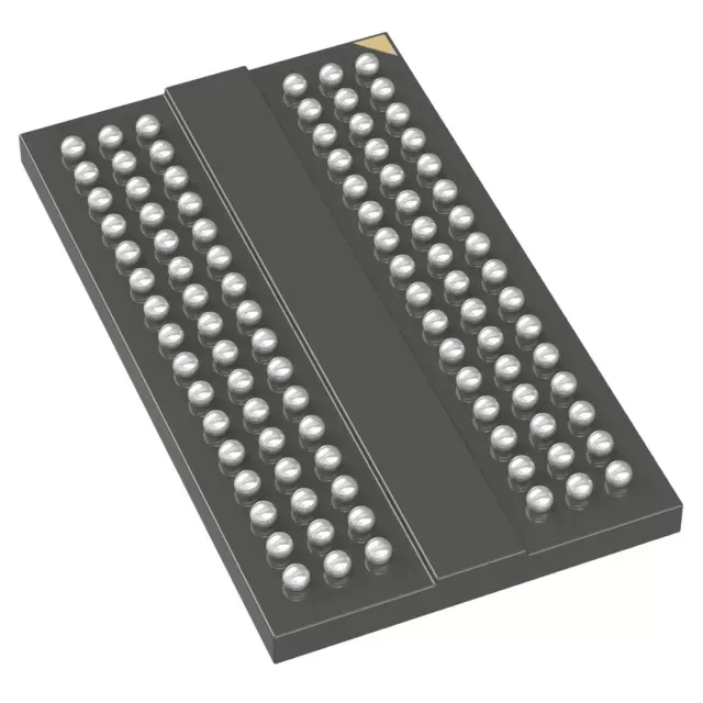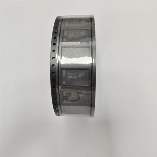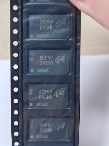
MT41K256M16TW-107:P
The MT41K256M16TW-107:P is a 4Gb DDR3L SDRAM from Micron Technology, organized as 256M words x 16 bits with a peak data rate of 1866 MT/s (DDR3-1866). Operating at the low-voltage 1.35V DDR3L standard, it delivers the same 1866 MT/s bandwidth as standard 1.5V DDR3 while consuming approximately 20% less power. The double data rate architecture with 8n prefetch, 8 internal banks, and programmable CAS latency (CL13 at -107 speed) make it ideal for embedded systems, industrial controllers, FPGA processing cards, and networking equipment where high memory bandwidth meets thermal/power constraints. The industry-standard 96-ball FBGA package ensures compatibility across a broad ecosystem of DDR3 memory controllers.
Product Specifications
MT41K256M16TW-107:P - Micron DDR3L SDRAM, 4Gb (256Mx16), 1866MT/s
Micron Technology - 4 Gbit, 1.35V Low-Voltage DDR3L, CL13, 8 Banks, 96-Ball FBGA 9x14mm
MFR Part #: MT41K256M16TW-107:PSuperb SKU: SUP-MT41K256M16TW-107:P
In Stock - Ready to Ship
The MT41K256M16TW-107:P is a 4Gb DDR3L SDRAM from Micron Technology, organized as 256M words x 16 bits with a peak data rate of 1866 MT/s (DDR3-1866). Operating at the low-voltage 1.35V DDR3L standard, it delivers the same 1866 MT/s bandwidth as standard 1.5V DDR3 while consuming approximately 20% less power. The double data rate architecture with 8n prefetch, 8 internal banks, and programmable CAS latency (CL13 at -107 speed) make it ideal for embedded systems, industrial controllers, FPGA processing cards, and networking equipment where high memory bandwidth meets thermal/power constraints. The industry-standard 96-ball FBGA package ensures compatibility across a broad ecosystem of DDR3 memory controllers.
Request QuoteContact Sales
Key Performance Highlights
Density / Organization
4 Gb / 256M x 16
Data Rate / Clock
1866 MT/s / 933 MHz
Supply Voltage
1.35 V DDR3L
CAS Latency
CL13 (13.91 ns)
Internal Banks
8 Banks
Package
96-FBGA (9 x 14 mm)
Technical Specifications
| Manufacturer | Micron Technology Inc. |
| Part Number | MT41K256M16TW-107:P |
| Memory Type | DDR3L SDRAM (Low-Voltage DDR3) |
| Density | 4 Gbit (512 MByte per chip) |
| Organization | 256M words x 16 bits |
| Speed Grade | -107 (DDR3-1866) |
| Data Rate | 1866 MT/s (million transfers per second) |
| Clock Frequency | 933 MHz |
| CAS Latency (CL) | CL = 13 (13.91 ns) |
| tRCD / tRP | 13.91 ns each (CL-tRCD-tRP = 13-13-13) |
| Architecture | Double Data Rate (DDR), 8n prefetch |
| Internal Banks | 8 (independent concurrent access) |
| Burst Length | 8 (fixed) or 4 (chopped) |
| Peak Bandwidth | ~3.73 GB/s per chip (x16, 1866 MT/s) |
| Supply Voltage | 1.35 V nominal (1.283 V - 1.45 V range) |
| Backward Compatible | Yes (can operate at standard DDR3 1.5V) |
| Auto Refresh | Self-refresh, auto-refresh (7.8 us interval) |
| Package | 96-ball FBGA (9 mm x 14 mm, 0.8 mm pitch) |
| Packaging | Tray |
| RoHS | RoHS Compliant (:P suffix = lead-free) |
Product Details
DDR3L Architecture & Power Efficiency
The MT41K256M16TW-107:P uses the DDR3L (Low-Voltage DDR3) standard, operating at 1.35V versus the traditional 1.5V DDR3. This delivers approximately 20% power savings at the same 1866 MT/s performance. The chip is backward-compatible with standard 1.5V DDR3 memory controllers.
8 Internal Banks: Concurrent bank access enables overlapping read/write operations, maximizing effective bandwidth. The 8n prefetch architecture reads 8 data words per clock cycle internally, feeding the double data rate I/O interface for sustained 1866 MT/s throughput on a 16-bit data bus.
Per-Chip Bandwidth: 16 bits x 1866 MT/s = ~3.73 GB/s peak. Using two x16 chips in parallel creates a 32-bit bus delivering ~7.46 GB/s. Four chips in a 64-bit configuration deliver ~14.9 GB/s — matching typical embedded CPU memory controller capabilities.
Key Applications
Embedded Computing - x86/ARM SBCs, COM Express modules, industrial PCs
FPGA Processing Cards - Xilinx Zynq, Altera SoC FPGA DDR memory expansion
Industrial Controllers - PLCs, CNC controllers, motion control systems
Networking Equipment - Routers, switches, base station controllers
Automotive Infotainment - Navigation systems, digital clusters, ADAS processing
Medical Imaging - Ultrasound, CT, MRI data acquisition buffers
Video Processing - Frame buffers, video walls, broadcast equipment
MT41K256M16TW Speed Grades
| Speed Code | Data Rate | Clock | CL | Peak BW (x16) | Use Case |
|---|---|---|---|---|---|
| -107 | 1866 MT/s | 933 MHz | 13 | 3.73 GB/s | Highest performance |
| -125 | 1600 MT/s | 800 MHz | 11 | 3.20 GB/s | General embedded |
| -187 | 1333 MT/s | 667 MHz | 9 | 2.67 GB/s | Cost-sensitive / legacy |
All three speed grades are pin-compatible (same 96-FBGA package) and can be used as drop-in replacements with corresponding memory controller reconfiguration.
Why Source MT41K256M16TW-107:P from Superb Automation?
Memory Subsystem BOM - DRAM + termination regulators + decoupling caps + connectors - one PO
DDR3 PCB Design - Length-matched, impedance-controlled 50-ohm routing, fly-by topology for address/command
BGA Assembly + X-Ray - 0.8mm pitch FBGA reflow with X-ray solder joint verification
Multi-Chip Configurations - 32-bit, 64-bit memory bus design support for dual and quad chip layouts
25 Years Trusted - Electronic components + PCBA partner since 2000
Genuine Parts - Direct from trusted Micron channels, full lot traceability
Frequently Asked Questions
What is the MT41K256M16TW-107:P used for?
This 4Gb DDR3L SDRAM serves as main memory in embedded computing, FPGA processing boards, industrial controllers, networking equipment, and automotive infotainment. Its 1866 MT/s speed and 1.35V low-voltage operation make it ideal where both performance and power efficiency matter.
What does -107 mean in the speed grade?
-107 = DDR3-1866, the fastest bin. -125 = DDR3-1600. -187 = DDR3-1333. The -107 grade operates at 933 MHz clock (1866 MT/s data rate) with CL13 latency. All three are pin-compatible and can be swapped by updating the memory controller timing parameters.
What is the difference between DDR3 and DDR3L?
DDR3L operates at 1.35V instead of 1.5V (standard DDR3), reducing power by ~20%. DDR3L chips are backward-compatible with 1.5V DDR3 controllers. The MT41K256M16TW-107:P can operate at either 1.35V (DDR3L mode) or 1.5V (standard DDR3 mode) for maximum design flexibility.
How much memory with multiple chips?
2 chips in x32 config: 8 Gbit (1 GB). 4 chips in x64 config: 16 Gbit (2 GB). Peak bandwidth scales: 2 chips = ~7.46 GB/s, 4 chips = ~14.9 GB/s. The 96-ball FBGA package enables dense PCB layouts for multi-chip memory arrays.
What does the :P suffix mean?
:P indicates lead-free (Pb-free) RoHS-compliant packaging. All current production Micron DRAM uses :P. The full ordering code includes temperature range (commercial, IT = -40 to +85C, AIT = -40 to +95C automotive, AUT = -40 to +125C) and packing type (TRAY vs TR for tape & reel).