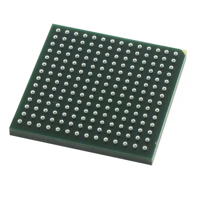

VBGQA1803
Brand: VBsemi
VBsemi VBGQA1803 is a discrete semiconductors component designed for AI Servers & Low-Altitude Economy (Drone and UAV) and related applications. In stock at Superb Automation — request a quote for competitive pricing and fast delivery.
Product Specifications
VBGQA1803
VBsemi — Discrete & Power Semiconductors
Product Overview
The VBGQA1803 from VBsemi is a discrete power semiconductor delivering efficient switching and power conversion. VBsemi (微碧半导体) specializes in discrete MOSFETs, power transistors, and protection devices for power supplies, motor control, and consumer electronics.
Superb Automation partners with leading brands including Qorvo, TI, ADI, XILINX, NVIDIA, Intel, ST, MACOM, Renesas, and Coilcraft to provide complete BOM and supply-chain solutions.
Key Features
- Low Rds(on) for minimal conduction losses in power switching
- Fast switching speed with low gate charge for high-frequency operation
- Avalanche-rated for robust operation under inductive load conditions
- High junction temperature rating for demanding environments
- Logic-level gate drive compatible for simplified design
- RoHS and AEC-Q101 qualified options available
Key Specifications
| Vds / Vce | V |
| Id / Ic | A |
| Rds(on) / Vce(sat) | mΩ |
| Qg | nC |
| Technology | — |
| Package | — |
| Configuration | — |
| Mounting | — |
Applications
Switch-Mode Power Supplies
Motor Drives & Inverters
Battery Management Systems
DC-DC Converters
Load Switching
Automotive Power Distribution
Request Quote — In Stock, 100% New & Original, Full Warranty
VBGQA1803: 80 V and 140 A in a 5 by 6 DFN
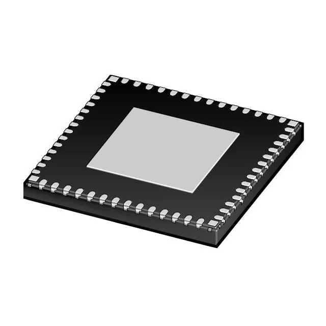
The VBGQA1803 is a single N channel MOSFET in a DFN8 body of 5 mm by 6 mm, rated at 80 V drain to source, plus or minus 20 V on the gate, a 3.5 V threshold, 140 A of drain current and 2.65 milliohm at a 10 V gate. The silicon is a shielded gate trench.
2.65 milliohm at 80 V in a surface mount body is a high current density. The die is large for a 5 by 6 pad, and the whole current has to spread across a pad about 4.5 mm by 5 mm before it reaches the copper. That is the constraint this part works against, and it is the reason a board that uses it looks different from one that uses a TO263 with the same resistance.
80 V is the class for a 48 V pack at the top of charge and for a 60 V PoE rail. At 2.65 milliohm a 30 A load loses 2.4 W, which a well built pad can remove without a heatsink, and a 60 A load loses 9.5 W, which it cannot.
Key data for the VBGQA1803
| Configuration | Single N channel |
| Package | DFN8, 5 mm by 6 mm, exposed pad |
| VDS | 80 V |
| VGS | Plus or minus 20 V |
| Vth | 3.5 V typical |
| ID | 140 A, a die figure at a 25 C case |
| RDS(on) at 10 V | 2.65 milliohm |
| Technology | Shielded gate trench |
| Loss at 20 A | 1.06 W through the channel |
| Loss at 40 A | 4.24 W through the channel |
| Body diode | Intrinsic, cathode at the drain |
| Thermal path | Pad, vias, and the copper planes around it |
Where 2.65 milliohm meets the pad
At 2.65 milliohm the die is below the resistance of the connection to it. The solder joint under a 5 by 6 pad is about 20 square millimetres, and a joint that thin contributes a share of a milliohm. The vias under the pad add more, and the copper that carries the current away from the pad is often the largest term in the sum.
That changes the way a board using this part should be checked. A thermal camera on the pad shows a hot spot at one edge where the current enters, not a uniform pad. The temperature that matters is the junction under that edge, and it is higher than the average the calculation gives.
It also changes the meaning of the 140 A column. The die can carry that current at a 25 C case, and the case cannot be at 25 C without a path that a 5 by 6 pad does not offer. For most products the honest continuous figure is between 25 and 50 A depending on the copper and the air.
There is a second order effect that decides whether the part works at all: the pad has to be flat and the solder has to be even. A 5 by 6 body with a large die is stiff, so a board that bows during reflow lifts one edge of the pad and the joint opens at the corner where the current enters. That failure looks like a resistance that rises after a few hundred thermal cycles, and it is found by cross sectioning rather than by an electrical test. The remedy is a board that stays flat through reflow, or a carrier, plus a pad a little larger than the joint needs rather than exactly the size of the body.
80 V for a 48 V pack: the margin question again
A 48 V lithium pack at the top of charge is about 58 V. An 80 V part derated to 80 per cent works to 64 V, which is 6 V above the top of charge. That is enough for a steady rail and thin for a transient, and it is the reason the 100 V class exists for the same application.
Where the transient comes from a load being removed from a long cable, the inductance puts a spike on the drain node and the switch sees it. A clamp across the switch or a suppressor at the connector is the usual answer, and it is cheaper than moving the whole line to 100 V.
Where the transient comes from regeneration, the bus rises and stays up for milliseconds, and a clamp cannot absorb it. That case needs either a brake or a higher voltage class, and no amount of resistance margin in the part will help.
Where the part fits and where it does not
It fits a 48 V battery disconnect, a synchronous rectifier on a 12 V or 24 V output fed from 48 V, a load switch on a 48 V bus at 20 to 40 A, a motor drive on a 36 V pack, and an ORing switch on a 48 V rail. It does not fit a 96 V pack, an automotive 48 V rail with load dump, or a continuous current above 50 A on a board without a heavy copper pad and airflow.
For a 48 V disconnect that has to hold its resistance over temperature, the parameters worth comparing are the resistance at the gate voltage in use and the way the current enters the pad. Our power management cross reference page covers how a candidate is compared with an original on the parameters that decide behaviour.
The sourcing side of this part is covered on the material requirements planning. For a 48 V switch used across several products, that page covers how demand is planned across builds.
Questions we get on this code
Can it replace a TO263 part with the same resistance? Electrically yes, thermally only if the pad and the vias match what the TO263 tab would have given. The footprint changes the answer more than the die does.
How much copper does the pad need? Enough that the spreading resistance is small against 2.65 milliohm, which means a plane on at least one inner layer and a dozen vias.
Does it need a gate resistor? A few ohms where the driver is fast, since a die this size rings on the drain at 48 V.
What should a purchase order carry? Part number, DFN8 5 by 6, and the reel quantity. We confirm the packing on the offer.