


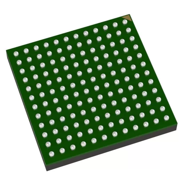

AD8330ACPZ
Brand: Analog Devices
Analog Devices AD8330ACPZ is a analog & mixed-signal component designed for Instrumentation and related applications. In stock at Superb Automation — request a quote for competitive pricing and fast delivery.
Product Specifications
AD8330ACPZ
Analog Devices — Analog & Mixed-Signal ICs
Product Overview
The AD8330ACPZ from Analog Devices is a high-performance analog / mixed-signal IC providing precision signal acquisition, conversion, and conditioning. Analog Devices (ADI) is a world leader in high-performance analog, mixed-signal, and DSP ICs for instrumentation, healthcare, automotive, and communications.
Superb Automation partners with leading brands including Qorvo, TI, ADI, XILINX, NVIDIA, Intel, ST, MACOM, Renesas, and Coilcraft to provide complete BOM and supply-chain solutions.
Key Features
- High-resolution data conversion with excellent SNR and THD
- Wide dynamic range and high linearity across operating conditions
- Integrated voltage reference with low temperature drift
- Flexible digital interface — SPI, I2C, or parallel options
- Industrial/automotive temperature range with guaranteed specs
- Low power consumption with power-down modes
Key Specifications
| Resolution | bits |
| Channels | — |
| Sample Rate | kSPS |
| Interface | — |
| Supply Voltage | V |
| Operating Temp | °C |
| Package | — |
| INL | LSB |
| SNR | dB |
| THD | dB |
Applications
Precision Instrumentation
Industrial Process Control
Medical Imaging & Diagnostics
Automotive Sensor Interfaces
Communications Infrastructure
Test & Measurement
Request Quote — In Stock, 100% New & Original, Full Warranty
AD8330ACPZ: 150 MHz at Every Gain Setting Is the Real Specification
The AD8330 is a DC to 150 MHz variable gain amplifier whose bandwidth does not move with gain. That single property separates it from most VGAs, where the gain bandwidth product is fixed and the bandwidth therefore falls as gain rises. A receiver that changes gain during a scan, an automatic gain control loop that rides a fading signal, or a pre converter stage that must hold its settling time across the whole range all depend on the bandwidth staying put, and this part is specified that way rather than by a gain bandwidth product.
Two gain interfaces, two different jobs
Gain can be set linearly in decibels, 0 dB to 50 dB for a control voltage from 0 V to 1.5 V, which is 30 mV per dB, or linearly in magnitude, where a magnitude control from 15 mV to 5 V gives a nominal gain from 0.03 to 10. The decibel interface suits a closed loop that integrates an error, because the loop gain stays constant in dB. The magnitude interface suits an open loop calibrated attenuator, because the gain is proportional to a voltage. The part also offers an inverted gain mode, 50 dB down to 0 dB at -30 mV per dB, which lets a single control line drive two stages in opposite directions.
Input range and what 0.3 mV means
Inputs are accepted from 0.3 mV rms to 1 V rms with rail to rail outputs, a differential input resistance of 1 kohm and an output resistance of 75 ohm per side. At maximum gain the input noise is 5 nV per root hertz typical. Over a 1 MHz band that is 5 uV rms, which is 1.7 percent of the 0.3 mV smallest specified input, so the part is not noise limited at its own bottom of range; it is limited by the 1 V rms top of range, where the output must still fit inside the rails with 75 ohm in series.
| Parameter | Value | What it decides |
|---|---|---|
| Bandwidth | 150 MHz at all gains | Settling time stays the same across the gain range |
| Gain, dB mode | 0 to 50 dB | 30 mV per dB from a 0 V to 1.5 V control |
| Gain, magnitude mode | 0.03 to 10 | Linear in voltage, 15 mV to 5 V control |
| Inverted mode | 50 dB down to 0 dB | -30 mV per dB, for a complementary control |
| Input range | 0.3 mV rms to 1 V rms | Three and a half decades of usable input |
| Input resistance | 1 kohm differential | Terminates a differential source without a transformer |
| Output resistance | 75 ohm per output | Drives a 75 ohm load with 150 ohm source |
| Input noise at maximum gain | 5 nV per root hertz | 5 uV rms over 1 MHz |
| Distortion | -62 dBc typical | Headroom against the converter behind it |
| Supply | 2.7 V to 6 V | One rail for both the core and the output stage |
| Supply current | 20 mA typical | 0.1 W at 5 V, 54 mW at 2.7 V |
| Offset compensation | Optional, on chip | Removes the DC term a high gain stage would amplify |
| Package | 3 mm by 3 mm LFCSP | Board area against the thermal path |
Offset and the reason the compensation pin exists
At 50 dB of gain, an input offset of 1 mV appears as 316 mV at the output, which is enough to consume a large part of a 5 V rail's output swing before any signal is applied. The on chip offset compensation removes that term, and it is the difference between a part that can be used at maximum gain and one that can only be used in the bottom half of its span. In a DC coupled chain the compensation also removes the offset of the preceding stage, which is usually the larger of the two.
Driving a converter and driving a cable
The 75 ohm output resistance is a deliberate match for video and cable loads, where a 75 ohm series element into a 75 ohm cable gives the correct source termination and a division by two. Into a high impedance converter input the same 75 ohm is a series resistance in front of the sampling capacitor, and it must be accounted for in the settling budget. The differential output can also be used single sided, but the second output then carries the common mode current and the even order terms no longer cancel.
Sourcing the exact grade
The order code fixes the package and the temperature range, and the datasheet figures above are attached to the part as a whole rather than to the cheapest grade. Where the same function is being bought as a second source, the parameters that must be compared are the constant bandwidth across gain, the input range and the output resistance, because a part with the same pin count and a different output resistance changes the load match. Availability of the listed codes is handled through amplifier cross reference, and the wider procurement route for this class of part is described in RF procurement. Where a board is being reworked around a short part, the verification steps are listed in how to verify a drop in replacement.