


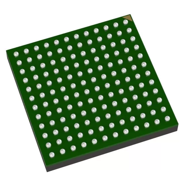

AD7799BRUZ
Brand: Analog Devices
Analog Devices AD7799BRUZ is a analog & mixed-signal component designed for Instrumentation and related applications. In stock at Superb Automation — request a quote for competitive pricing and fast delivery.
Product Specifications
AD7799BRUZ
Analog Devices — Analog & Mixed-Signal ICs
Product Overview
The AD7799BRUZ from Analog Devices is a high-performance analog / mixed-signal IC providing precision signal acquisition, conversion, and conditioning. Analog Devices (ADI) is a world leader in high-performance analog, mixed-signal, and DSP ICs for instrumentation, healthcare, automotive, and communications.
Superb Automation partners with leading brands including Qorvo, TI, ADI, XILINX, NVIDIA, Intel, ST, MACOM, Renesas, and Coilcraft to provide complete BOM and supply-chain solutions.
Key Features
- High-resolution data conversion with excellent SNR and THD
- Wide dynamic range and high linearity across operating conditions
- Integrated voltage reference with low temperature drift
- Flexible digital interface — SPI, I2C, or parallel options
- Industrial/automotive temperature range with guaranteed specs
- Low power consumption with power-down modes
Key Specifications
| Resolution | bits |
| Channels | — |
| Sample Rate | kSPS |
| Interface | — |
| Supply Voltage | V |
| Operating Temp | °C |
| Package | — |
| INL | LSB |
| SNR | dB |
| THD | dB |
Applications
Precision Instrumentation
Industrial Process Control
Medical Imaging & Diagnostics
Automotive Sensor Interfaces
Communications Infrastructure
Test & Measurement
Request Quote — In Stock, 100% New & Original, Full Warranty
AD7799BRUZ: 27 nV of Noise From a Part That Draws 380 uA
The AD7799 is a 24 bit sigma-delta converter with three differential inputs, an on chip instrumentation amplifier, an internal clock oscillator and a supply current of 380 uA typical from 2.7 V to 5.25 V. At a gain of 64 and a 4.17 Hz update rate the rms noise is 27 nV, and at 16.7 Hz it is 65 nV. Power-down current is 1 uA maximum, the update rate is programmable from 4.17 Hz to 470 Hz, and the part includes a low side power switch, burnout current sources and programmable digital outputs.
Milliwatts against nanovolts
At 3 V and 380 uA the part draws 1.14 mW, which for a 24 bit converter with an input amplifier is a battery instrument figure rather than a bench instrument figure. The noise of 27 nV at a gain of 64 on a 2.5 V reference corresponds to a differential span of 78.1 mV and a code size of 4.66 nV, so 27 nV is 5.8 codes rms, about 19 noise-free bits. That is enough for a 2000 count weighing scale with a factor of a hundred in reserve, and it is achieved without an external amplifier.
What the burnout current sources are for
A broken sensor on a bridge or a thermocouple produces an open circuit, and an open circuit into a high impedance input produces a reading that looks like a valid signal. The burnout current sources inject a small current into the input, so an open sensor drives the reading to full scale instead of leaving it floating. This turns a silent failure into a detectable one, and it is the kind of feature that separates a converter for instrumentation from a converter for data acquisition.
| Parameter | Value | What it decides |
|---|---|---|
| Resolution | 24 bit, AD7799 | 16 bit on the AD7798 with the same pinout |
| Channels | Three differential | A bridge plus two auxiliary sensors |
| RMS noise at 4.17 Hz | 27 nV at gain 64 | 5.8 codes on a 78.1 mV span |
| RMS noise at 16.7 Hz | 65 nV at gain 64 | Four times the rate, 2.4 times the noise |
| Update rate | 4.17 Hz to 470 Hz | Speed traded against noise in one register |
| Supply current | 380 uA typical | 1.14 mW at 3 V |
| Power-down current | 1 uA maximum | Two decades below the active state |
| Supply | 2.7 V to 5.25 V | Two cells or a 3 V rail |
| Interface supply | Independent | A 3 V converter on a 5 V analog rail |
| Line rejection | 50 Hz and 60 Hz | Both frequencies rejected together |
| Diagnostics | Burnout currents, reference detect | An open sensor becomes a readable fault |
| Outputs and switch | Programmable digital outputs, low side switch | Drives an excitation path without extra parts |
| Package | 16-lead TSSOP | Small for a complete front end |
Four times the rate costs 2.4 times the noise
Going from 4.17 Hz to 16.7 Hz raises the rms noise from 27 nV to 65 nV, which is a factor of 2.4 rather than the factor of two that a pure white noise argument would give. The extra comes from the digital filter's shape and from the 1/f component of the amplifier. The practical consequence is that a system needing 60 Hz rejection at 50 Hz update rate has to accept roughly the 16.7 Hz noise figure, because the filter that rejects the line frequency is the slower one.
The low side switch and the excitation
The low side power switch lets the converter interrupt the bridge excitation between readings, which removes the DC offset of the bridge from the measurement and halves the self heating. A switched excitation scheme with two readings, one with the excitation on and one with it off, subtracts the offset and the amplifier's own offset in the same operation. That technique depends on the switch being on the low side, which is why the feature exists in this part rather than as an external transistor.
Buying an instrument front end
The comparison across candidates is rms noise at the intended update rate, the gain range and the diagnostic features, and the order code fixes the resolution grade. A part with the same package and a lower price but no burnout source cannot detect an open sensor. Availability is tracked through ADC DAC cross reference, and the wider supply question for a portable instrument is set out in one stop BOM sourcing. Where the original code is short, the options are in obsolete part cross reference hub.