

Converters are replaced more often than most analogue parts. A data converter family is retired when a fab line closes, and a faster device with a familiar part number appears every few years, so an ADC DAC cross reference is one of the most frequent requests that reaches a sourcing desk.
The request looks simple: same resolution, same sample rate, same package. The failures appear later, in the digital interface, in the reference, and in the timing that the rest of the board was built around.
Where converter cross references fail
The first failure is the interface. Two converters can both be 14 bit parts in the same QFN, while one presents parallel CMOS and the other a serial lane interface with an embedded clock. The analogue side may be equivalent and the digital side becomes a different FPGA pinout, a different capture block, and a different latency through the signal chain.
The second failure is the reference. A converter with an internal reference looks easier to use until the replacement reference is noisier or drifts more, and a measurement that used to hold over temperature starts to walk. The third is the analogue front end: input bandwidth, input impedance and the drive needed at the sampling instant decide whether the existing transformer or amplifier can still drive the part.
Then there is timing. Pipeline delay, deterministic latency and the clock jitter budget are rarely in the headline specification, and they are exactly what a control loop notices.
The parameters that decide an ADC DAC cross reference
| Parameter | Why it decides the outcome | What a weak comparison looks like |
|---|---|---|
| Resolution and linearity | INL and DNL, missing codes and noise floor define the usable bits in the application | Same resolution quoted, two effective bits lost at the top of the band |
| Sample or update rate | Sets the bandwidth the converter can carry, and the clock the board has to deliver | Rate matched on paper, clock jitter budget not compared |
| Digital interface | Parallel, LVDS or serial lanes decide pin count, capture logic and latency | Same package, different protocol, so the receiving device needs new logic |
| Analogue input | Bandwidth, impedance and common mode decide what can drive the part | Datasheet bandwidth matched, existing front end cannot settle in time |
| Reference | Internal or external, with noise and drift that set long term accuracy | Reference assumed equivalent, accuracy drifts over temperature |
| Supply rails and sequencing | Rail count, order and decoupling decide whether it starts cleanly every time | Rails matched in value, sequencing not compared, occasional start up fault |
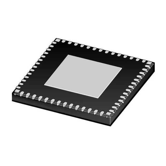
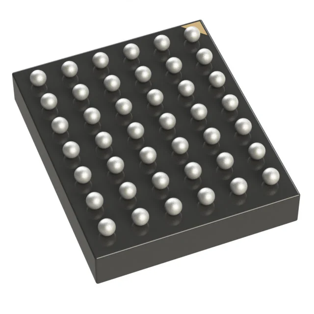
| Package and thermal pad | Footprint, pin rotation and pad geometry decide whether the board can be reused | Same body size, pad and pin map different, so a new board is needed anyway |
| Grade and status | Temperature grade, screening and how long the brand will keep the part in production | Commercial grade where the build needs industrial screening |
How SUPERB PCBA handles a converter change
Send the original part number, the board it sits on and the quantity per year. The reply is a line by line comparison against the table above, with the interface, reference and timing differences written out, and with any point the datasheet does not settle returned as a question plus the condition that closes it. Where the original is end of life, the routes are collected in the obsolete part cross reference hub. The devices themselves sit under power management and signal chain and analogue and mixed signal ICs, so a candidate can be checked against the families already listed.
Provenance is checked before a replacement enters a build. Reels are counted by X-ray, packages and markings are inspected, and decapsulation is used where the risk justifies it. Verified lots carry a 730 day warranty, and a substitution only enters the BOM after written approval from your side. For candidates that are pin compatible on paper, the procedure in pin to pin cross reference is used to confirm the pin map before anything is ordered.
SUPERB Assembly then proves the change on hardware: first article inspection against released data, fine pitch placement down to 01005, 3D SPI before reflow and 3D AOI after it, X-ray inspection in 2D and CT mode with voiding below 5 percent, in circuit and functional test on fixtures approved by your team, under IPC-A-610 Class 2 and Class 3, IPC-7095 for area array work, ISO 9001, and ISO 13485 for medical programmes. Boards in the same build are supported from 500 MHz to 77 GHz with lines down to 0.05/0.05 mm, impedance held to plus or minus 5 percent and to plus or minus 2 percent where the circuit needs it, and up to 68 layers, which covers the RF converter boards used in test and instrumentation work as well as the mixed signal control boards.
Where the interface has to change, the board change stays inside the same order, so the new capture routing, the reference decoupling and the converter are qualified together instead of arriving from three directions. SUPERB Tech keeps the comparison, the approval and the test data against the build, so the next audit or the next revision starts from a record rather than a memory.
When the interface is the real change
A serial lane interface is the common case. The replacement may need fewer pins and a higher line rate, which sounds like an improvement until the receiving device is checked: the lane count, the reference clock, the deterministic latency and the equalisation settings all move. The board change itself can be small, while the capture logic and the test plan carry most of the work.
This is why the comparison is written before the sample is ordered. A candidate that saves a connector and costs three weeks of bring up is not a saving, and the difference is visible at the comparison stage rather than after the first build.
ADC DAC cross reference questions
Can a converter with a higher sample rate always replace a slower one?
Only if the interface, the reference and the clocking are compatible. A faster device that changes the interface costs more in bring up than it returns in headroom.
Is an internal reference always easier than an external one?
It is simpler to lay out, not necessarily more accurate. Reference noise and drift decide the answer, and both have to be compared for the temperature range the product sees.
How is a converter replacement proved?
On the board, with first article inspection, functional test and, where the programme requires it, a check at the temperature corners. The comparator table is the starting point, not the evidence.
What if the replacement needs new capture logic?
The change is quoted with the board and the test plan so the cost is known at the decision. Where the receiving device cannot support the new interface, a different candidate is found instead.
Next step
Send the original converter part number, the board it belongs to and the quantity per year. You get the comparison with the interface, reference and timing differences marked, the candidate list with availability, and the test plan needed to release the change.