


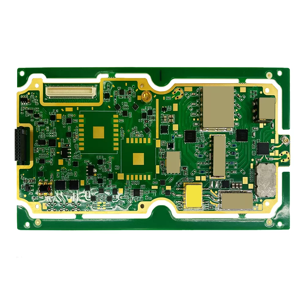

TMS320F28374SPTPT
Brand: Texas Instruments
Texas Instruments TMS320F28374SPTPT is a power management component designed for AI Servers & Low-Altitude Economy (Drone and UAV) and related applications. In stock at Superb Automation — request a quote for competitive pricing and fast delivery.
Product Specifications
TMS320F28374SPTPT
Texas Instruments — Power Management & Signal Chain
Product Overview
The TMS320F28374SPTPT from Texas Instruments is a power management / signal chain IC delivering high efficiency, precision regulation, and robust protection. Texas Instruments (TI) is a global leader in analog ICs, power management solutions, and embedded processors.
Superb Automation partners with leading brands including Qorvo, TI, ADI, XILINX, NVIDIA, Intel, ST, MACOM, Renesas, and Coilcraft to provide complete BOM and supply-chain solutions.
Key Features
- High-efficiency power conversion with low quiescent current
- Wide input voltage range with precision output regulation
- Integrated over-current, over-temperature, and short-circuit protection
- Small footprint packaging for space-constrained designs
- AEC-Q100 qualified options available for automotive applications
- Flexible sequencing and soft-start control
Key Specifications
| Input Voltage | V |
| Output Voltage | V |
| Output Current | A |
| Switching Frequency | kHz |
| Efficiency | % |
| Quiescent Current | µA |
| Topology | — |
| Package | — |
| Operating Temp | °C |
| Protection | — |
Applications
Industrial Automation
Automotive Electronics
Telecom Infrastructure
Server & Data Center Power
Medical Devices
Consumer Electronics
Request Quote — In Stock, 100% New & Original, Full Warranty
TMS320F28374SPTPT single core real time controller with 512 kilobytes of flash in the 176 pin body
The TMS320F28374SPTPT is a member of the F2837xS family in the 176 pin thermally enhanced low profile quad flat pack, with 512 KB of error corrected flash and 132 KB of RAM. The core is the C28x at 200 MHz with a floating point unit, a trigonometric math unit and a control law accelerator running at the same clock, and the analog section carries the same converters and comparators as the rest of the family.
The reason to choose this member rather than the larger ones is memory. A product that needs the analog count, the PWM channels and the USB port of the family but can live with half the flash and less RAM saves cost without changing the board, because the body and the pinout are shared. The suffix chain reads PTP for the 176 pin body and T for the minus 40 to plus 105 C junction grade, which is the grade below the top of the family range.
Key parameters taken from the TMS320F28374SPTPT document
| Core | C28x at 200 MHz with a single precision floating point unit, trigonometric math unit and VCU-II |
| Co processor | control law accelerator at 200 MHz, runs floating point code independently of the CPU |
| Flash | 512 KB, error correction code protected |
| RAM | 132 KB total, with 96 KB of global shared RAM in this member |
| Analog | four 16 bit converters in the family, 1.1 MSPS each and 4.4 MSPS system throughput, differential inputs |
| PWM | 24 channels with enhanced features and high resolution outputs |
| Capture and position | six enhanced capture modules, three enhanced quadrature encoder modules |
| Serial | USB 2.0 with MAC and PHY, CAN, SPI, SCI, I2C and McBSP ports |
| Memory interface | external memory interfaces with ASRAM and SDRAM support |
| Package | HLQFP PTP, 176 pins, 40 parts per JEDEC tray |
| Order code facts | TMS320F28374SPTPT, Active, minus 40 to plus 105 C per the T suffix |
| Family position | same body and pinout as the larger F2837xS members, with less flash and RAM |
The table above is read from the vendor document, not from a distributor summary. Where a window is printed, the window is what a production test should use, and the typical value is only a starting point for the first article.
Where the numbers matter in a real build
The memory difference is where the porting work hides. Moving from a 1 MB member to this one changes the linker command file, the sector allocation for the field update path and the size of any RAM buffer used for a trace or a communication stack. The peripheral addresses and the pin functions do not change, which is what makes the substitution attractive, but a firmware image that was built for 1 MB will simply not fit, and the first sign is usually a linker error late in a release cycle.
The 132 KB of RAM on this member splits differently from the larger ones, with 96 KB of global shared RAM against 128 KB on the top members. On a control application that uses the shared RAM for communication buffers and a trace, that reduction is the number to check before the substitution. A program that runs at 80 percent RAM use on the larger member will not link here.
The T suffix sets the junction range at minus 40 to plus 105 C. That is adequate for most industrial enclosures but it is not the top of the family, and a product that runs a 200 MHz core with all four converters active in a sealed box will approach it. The grade has to be chosen from a measured case temperature in the target enclosure, and the measurement has to be taken with the real firmware running rather than with a test loop.
The analog section is unchanged from the rest of the family, so the same rules apply. Four converters at 1.1 MSPS each give 4.4 MSPS of system throughput only when the sample windows are short and the drive impedance is low. The hardware post processing block that averages and thresholds conversions exists to keep the CPU out of that path, and it should be configured during bring up rather than left for an optimisation pass.
Because the board and the pinout are shared, this part is also the natural second source inside a product family. A build that has been qualified on the larger member can be moved to this one without touching the board, which is a supply continuity option rather than a cost reduction. The vendor addendum lists this code as Active in the same body, so both can be held on one approval.
- The 176 pin body keeps the full pin set, so a substitution from a larger member does not change the board.
- 512 KB of flash is enough for a control application with a dual image update path if the images are sized at build time, not at the end of the project.
- Three encoder modules and six capture inputs cover a multi axis drive with home switches without using CPU pins.
- Four converters at 1.1 MSPS each allow simultaneous sampling of three phase currents plus a direct current link channel.
- The 105 C junction grade sets the thermal ceiling, and it is the number to compare against a measured case temperature rather than against an ambient estimate.
The first article check should confirm the flash image size against the sector map, the shared RAM left free under the communication stack and the trace buffer, and the junction temperature at the worst simultaneous sampling case. On a substitution from a larger member, the first two are the numbers that decide whether the change is safe, and the third decides whether the grade is high enough. Write the three readings into the build record for every lot, because a substitution is only safe while they stay inside the window.
Which projects this part fits
Three phase drives, servo amplifiers, solar and storage converters, charger modules, industrial power supplies, robotics controllers and instrument front ends that need simultaneous sampling all fit this member. It is also the substitution candidate when a product built on a larger F2837xS part is under cost pressure, because the board does not change. Our MCU cross reference lists what we hold against this family, and the incoming inspection plan page sets out the receiving checks on a 176 pin tray.
Questions that come up before a purchase order is released
Does this part need a different board from the larger family members?
No. The body, the pinout and the peripheral addresses are shared, so one board can carry either. What changes is the memory map, and the firmware has to be rebuilt with a linker command file that matches the smaller flash and RAM.
Which temperature grade is this?
The T suffix is minus 40 to plus 105 C junction. The family also offers a higher grade under another suffix in the same body, so a product that runs hot should compare the two before the reel is ordered.
How much flash does the application actually get?
The full 512 KB array is available to the application apart from the reserved sectors used for calibration and the boot configuration. The sector map in the family document should be used to place the boot image and the parameter store rather than letting the linker place them by size.
How SUPERB handles this line
We supply the TMS320F28374SPTPT in original trays with date code and lot traceability, and we can supply it alongside the larger members of the same family so that one approval covers a supply option. If the product is being moved down from a bigger part, send the memory map and the flash use and we will confirm that the image fits before the change is released. Start from the component lead time solutions page if the question is schedule rather than cost.


