
VBL16I25S
Brand: VBsemi
VBsemi VBL16I25S is a discrete semiconductors component designed for AI Servers & Low-Altitude Economy (Drone and UAV) and related applications. In stock at Superb Automation — request a quote for competitive pricing and fast delivery.
Product Specifications
VBL16I25S
VBsemi — Discrete & Power Semiconductors
Product Overview
The VBL16I25S from VBsemi is a discrete power semiconductor delivering efficient switching and power conversion. VBsemi (微碧半导体) specializes in discrete MOSFETs, power transistors, and protection devices for power supplies, motor control, and consumer electronics.
Superb Automation partners with leading brands including Qorvo, TI, ADI, XILINX, NVIDIA, Intel, ST, MACOM, Renesas, and Coilcraft to provide complete BOM and supply-chain solutions.
Key Features
- Low Rds(on) for minimal conduction losses in power switching
- Fast switching speed with low gate charge for high-frequency operation
- Avalanche-rated for robust operation under inductive load conditions
- High junction temperature rating for demanding environments
- Logic-level gate drive compatible for simplified design
- RoHS and AEC-Q101 qualified options available
Key Specifications
| Vds / Vce | V |
| Id / Ic | A |
| Rds(on) / Vce(sat) | mΩ |
| Qg | nC |
| Technology | — |
| Package | — |
| Configuration | — |
| Mounting | — |
Applications
Switch-Mode Power Supplies
Motor Drives & Inverters
Battery Management Systems
DC-DC Converters
Load Switching
Automotive Power Distribution
Request Quote — In Stock, 100% New & Original, Full Warranty
VBL16I25S: a 600 V IGBT with its diode in a TO263
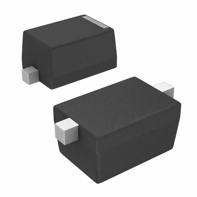
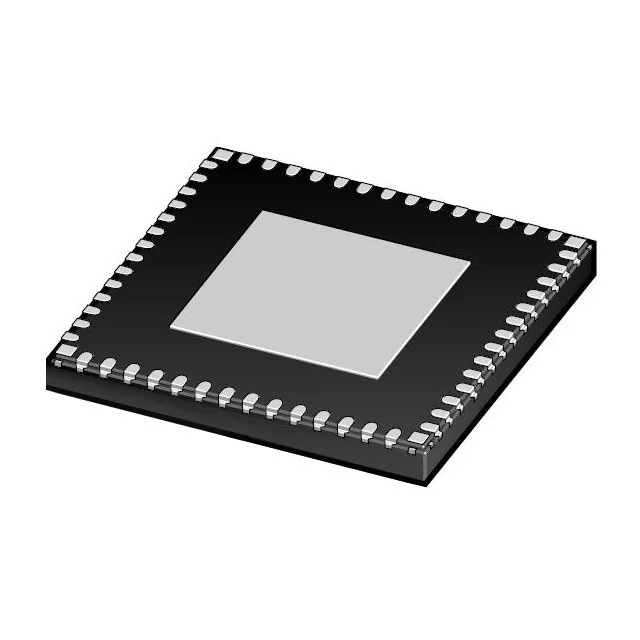
The VBL16I25S is an insulated gate bipolar transistor with a co-packaged fast recovery diode in a TO263 body, the surface mount package also sold as D2PAK. Collector to emitter is 600 V, the class sheet prints 650 V at the top of the range, gate to emitter is plus or minus 20 V, the gate threshold is 5 V, continuous collector current is 25 A and saturation voltage is 1.9 V with 15 V on the gate. The die is listed as SJ.
This is a switch for a high voltage rail, not for a low voltage one. At 600 V it holds a 400 V DC bus with the usual margin and it holds a 230 V AC line after rectification at about 325 V with room for the transient. It does not hold a 480 V AC line at 680 V after rectification, which belongs to the 1200 V class, and it does not hold a 400 V bus during a regeneration event that lifts the rail above 600 V without a clamp.
Nothing about this part reads like a MOSFET. There is no on resistance to multiply by the square of the current, because the forward drop is roughly constant once the device is on. That single fact changes the loss arithmetic, the thermal arithmetic and the way the part is chosen.
Key data for the VBL16I25S
| Package | TO263, surface mount with the tab on the collector |
| Configuration | IGBT with a co-packaged fast recovery diode |
| VCE | 600 V, printed as 600/650 at the top of the class |
| VGE | Plus or minus 20 V |
| VGEth | 5 V, which is not a logic level gate |
| ICE | 25 A, a die figure at a 25 C case |
| VCEsat at 15 V | 1.9 V |
| Technology | SJ |
| Loss at 5 A | 9.5 W at 1.9 V |
| Loss at 10 A | 19 W at 1.9 V |
| Loss at 25 A | 47.5 W at 1.9 V |
| Gate drive needed | 15 V on, and a negative or zero bias off with a hard pull down |
Reading the saturation figure as a loss
At 1.9 V and 10 A the device turns 19 W into heat inside the die. At the printed 25 A it turns 47.5 W into heat. A TO263 tab soldered to a copper island removes a few watts in still air and perhaps fifteen with a large area, vias and airflow, so the printed current is a die rating that the body cannot carry in a real product.
The working current falls out of the loss the board can remove. At 5 A the part makes 9.5 W, which a generous copper island can hold with a case around 100 C. At 3 A it makes 5.7 W, which is comfortable. For a continuous load near the printed 25 A the answer is not this package at all, it is a TO247 with a heatsink, or several devices in parallel with emitter resistors to share the current.
Switching loss sits on top of that. The part has to cross the linear region at every transition, and at 20 kHz with a hard turn off the transition loss can match the conduction loss at half load. That is the reason a part like this belongs in a converter below about 30 kHz or in a circuit where the switch is on for most of the period.
What the 5 V threshold means for the driver.
A 5 V threshold is the standard for this class and it rules out driving the gate from a logic output. The gate needs about 15 V to reach the printed saturation, and the usual driver is a dedicated gate drive transformer or an isolated driver with a 15 V rail and a separate negative rail for the off state.
The plus or minus 20 V window is comfortable for a 15 V drive but it leaves only 5 V of headroom on the positive side. Gate loop ringing on a fast turn off can swing above that, so the gate resistor and the loop area matter as much as they do on a MOSFET. A 10 to 33 ohm resistor at the gate, a short return to the emitter and a transient suppressor across the gate are the usual protection.
Miller turn on is the other hazard. When the diode in the opposite leg recovers, the collector to gate capacitance pulls the gate up, and a gate held at zero volts through a weak resistor can see a pulse high enough to turn the device partly on, which puts both devices of a bridge leg on at the same time. A negative off bias of 5 to 8 V is the normal answer, and it is the reason many drivers are specified with a bipolar output.
The diode is not a spare part
The co-packaged diode is there because an IGBT cannot conduct in reverse. In a bridge leg or a flyback the current has to flow the other way for part of the period, and the diode inside the package provides that path with the shortest possible loop. It also means the reverse recovery charge of that diode appears as a loss in the opposite device at every commutation.
On a 600 V part the diode recovery is soft enough for most converters but it is not free. At 20 kHz and 10 A the recovery loss can be a few watts, and it rises with temperature and with the rate of fall of the current. Two things help: keep the switching frequency low, and keep the loop between the diode and the opposite switch short, because loop inductance turns recovery into a voltage spike rather than a loss.
Where the part runs in a bridge, the diode also sets the dead time. Too little dead time and the diode conducts, then the other device turns on into a recovered junction, which is where the largest spike comes from. Too much dead time and the diode carries current for longer than it should, which is a loss in a part that does not need to be warm.
Where the part fits and where it does not
It fits a front end power factor stage below 30 kHz, an induction heating driver, a small welder, a brake chopper on a 400 V bus, the primary switch of a low frequency flyback in a charger and a clamp in a motor drive. It does not fit a 100 kHz converter, a 480 V AC input without a 1200 V device, or a load near the printed current in a TO263 body.
For a 600 V front end the two figures that decide between candidates are the saturation voltage at the working current and the thermal path the board offers. Our power management cross reference page covers how a candidate is compared with an original on the parameters that decide behaviour rather than on the headline current.
The sourcing side of this part is covered on the incoming inspection plan. For a 600 V switch bought in lots, that page covers what is measured before the parts reach the line.
Questions we get on this code
Can the gate be driven from a 5 V logic output? No. The threshold is 5 V, so a 5 V output sits at the edge of conduction and the device would run in its linear region. It needs about 15 V, which means a driver and often an isolated supply.
Is 25 A available continuously? Not in this body. 47.5 W at the printed current has nowhere to go. Work back from the copper and expect a few amps continuous, or move to a larger package.
Does the part include the freewheel diode? Yes, and that is the point of the product. The diode is fast recovery and matched to the die, which keeps the commutation loop short.
What should a purchase order carry? Part number, TO263, and the packing the line can take. We confirm the reel quantity on the offer rather than assuming it.