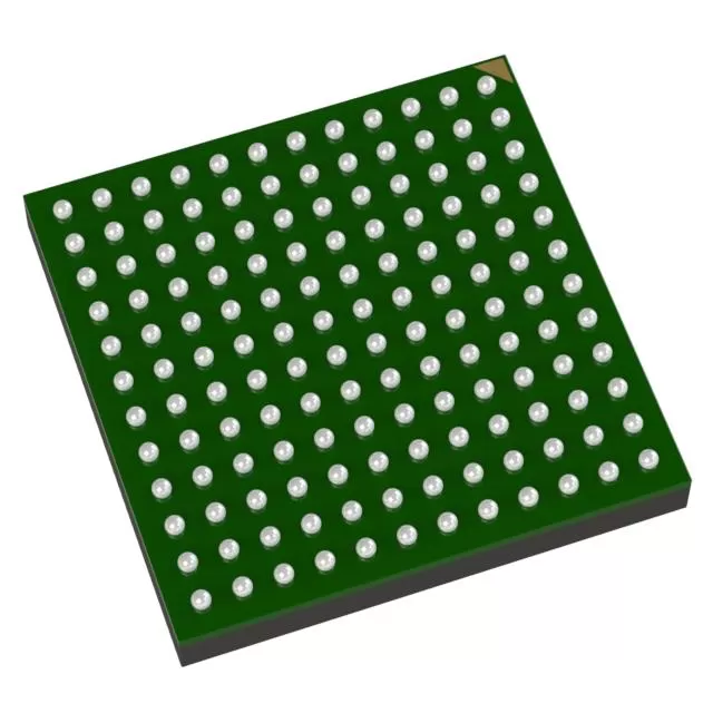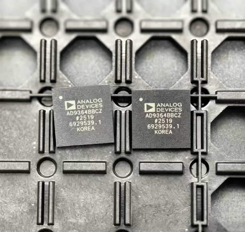

HMC8205BF
Brand: Analog Devices
Analog Devices HMC8205BF is a analog & mixed-signal component designed for Instrumentation and related applications. In stock at Superb Automation — request a quote for competitive pricing and fast delivery.
Product Specifications
HMC8205BF
Analog Devices — Analog & Mixed-Signal ICs
Product Overview
The HMC8205BF from Analog Devices is a high-performance analog / mixed-signal IC providing precision signal acquisition, conversion, and conditioning. Analog Devices (ADI) is a world leader in high-performance analog, mixed-signal, and DSP ICs for instrumentation, healthcare, automotive, and communications.
Superb Automation partners with leading brands including Qorvo, TI, ADI, XILINX, NVIDIA, Intel, ST, MACOM, Renesas, and Coilcraft to provide complete BOM and supply-chain solutions.
Key Features
- High-resolution data conversion with excellent SNR and THD
- Wide dynamic range and high linearity across operating conditions
- Integrated voltage reference with low temperature drift
- Flexible digital interface — SPI, I2C, or parallel options
- Industrial/automotive temperature range with guaranteed specs
- Low power consumption with power-down modes
Key Specifications
| Resolution | bits |
| Channels | — |
| Sample Rate | kSPS |
| Interface | — |
| Supply Voltage | V |
| Operating Temp | °C |
| Package | — |
| INL | LSB |
| SNR | dB |
| THD | dB |
Applications
Precision Instrumentation
Industrial Process Control
Medical Imaging & Diagnostics
Automotive Sensor Interfaces
Communications Infrastructure
Test & Measurement
Request Quote — In Stock, 100% New & Original, Full Warranty
HMC8205BF10: 0.3 GHz to 6 GHz at 35 W, in a package that cannot go through reflow
The HMC8205BF10 is a gallium nitride broadband power amplifier in a 10-lead ceramic leaded chip carrier that delivers 45.5 dBm, or 35 W, across 0.3 GHz to 6 GHz from a 50 V drain supply at 1300 mA quiescent. It needs no external matching and no external bias inductor, and the dc blocking capacitors are inside the package. The constraint that shapes every assembly using it is that the body is not surface mountable and cannot pass a solder reflow.
Published values
| Parameter | Value |
|---|---|
| Frequency range | 0.3 GHz to 6 GHz instantaneous |
| Saturated output power | 46 dBm at 0.3 to 3 GHz, 46 dBm at 3 to 6 GHz |
| Compressed output power, 4 dB | 45 dBm typical |
| Small signal gain, 0.3 to 3 GHz | 23 dB minimum, 26 dB typical |
| Small signal gain, 3 to 6 GHz | 25 dB minimum, 28 dB typical |
| Power gain at saturation | 20 dB, 0.3 to 3 GHz |
| Power added efficiency | 38% at 0.3 to 3 GHz, 35% at 3 to 6 GHz |
| Drain supply | 50 V nominal, 28 V to 55 V, 60 V absolute maximum |
| Quiescent current | 1300 mA |
| Gate supply | -8 V to 0 V |
| Input drive, absolute maximum | 35 dBm |
| Package | 10-lead LDCC, flange mounted, not reflow compatible |
The 45.5 dBm and 46 dBm on the same page
The general description states 45.5 dBm, or 35 W, while the specification table states 46 dBm saturated. The difference is 0.5 dB, which is inside the measurement uncertainty of a pulsed power measurement at this level but is not zero, and a link budget should use the lower of the two unless the higher has been measured on the actual board.
45.5 dBm is 35.5 W and 46 dBm is 39.8 W, so the two statements differ by about 4 W. For a system that is specified at 30 W output the difference does not matter. For one specified at 38 W it is the difference between passing and failing, and the honest answer is that the module has to be measured.
Current, efficiency and the 1300 mA
46 dBm at 38 percent efficiency implies about 105 W of dc input, which at 50 V is 2.1 A. The 1300 mA in the specification is the quiescent current, so the supply, the connectors and the bulk capacitance all have to be sized for roughly twice that. At 28 V the same output needs 3.7 A, which is why the part is normally run at 50 V.
The gate is adjusted between -8 V and 0 V to set the quiescent current, and the drain absolute maximum is 60 V, so a 50 V rail with a 20 percent transient is at the limit. A rail that is allowed to overshoot on load dump will take the part with it, and a transient suppressor on the drain is cheaper than a replacement amplifier.
No external matching, and what that saves
No external matching means the 50 ohm ports are set inside the package across the whole 0.3 GHz to 6 GHz band, and no bias inductor is needed because the bias network is internal. For a broadband jammer or a general purpose amplifier that removes a tuning exercise that would otherwise have to cover five octaves, which no single external network does well.
The dc blocking capacitors are internal too, so the ports are dc isolated and a source with a dc offset does not have to be protected against. That is one fewer component per port and one fewer way to get the assembly wrong.
Assembly, which is where this part differs
The datasheet states that the device is not surface mountable, is not intended for a solder reflow process, and must not be exposed to an ambient above 150 C. It is a flange mounted carrier that is screwed to a heatsink and connected with ribbon bonds or solder preforms, and the radio frequency launch is part of the mechanical assembly.
For a programme used to reflow assemblies this changes the process flow: the amplifier is fitted after the board is populated, by hand or in a separate operation, and the thermal interface between the flange and the heatsink becomes a specification item. Thermal grease, a gap pad or a solder preform each give a different junction temperature for the same flange temperature.
When an order code in this family cannot be found, the amplifier cross reference lists what else does the same job, defense grade components covers what to check before a part is dropped into an existing board, and component lead time solutions is the route we take on a live shortage.
Two questions buyers ask
Is the HMC8205BF10 a 35 W or a 40 W part? The general description says 45.5 dBm, which is 35 W, and the specification table says 46 dBm, which is 39.8 W saturated. Use the lower figure for a budget and measure the module for the higher.
Can it be soldered in a reflow oven? No. The vendor states the device is not surface mountable and is not suitable for a solder reflow process, with a 150 C maximum ambient. It is flange mounted to a heatsink and connected by ribbon bond or solder preform.