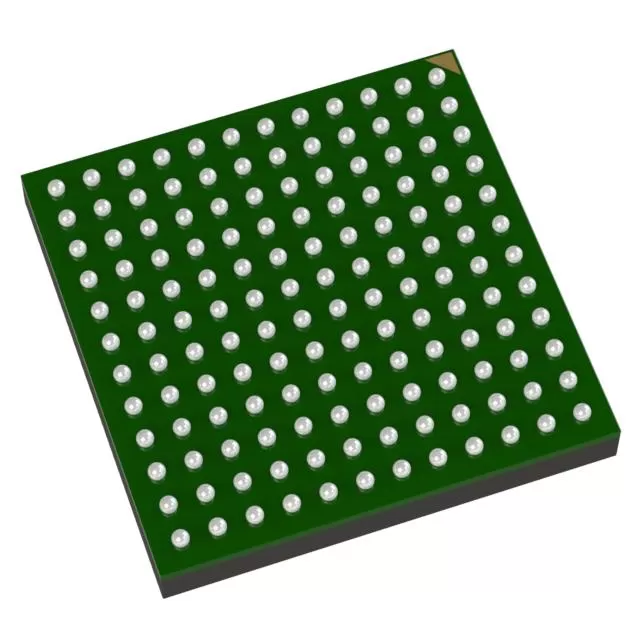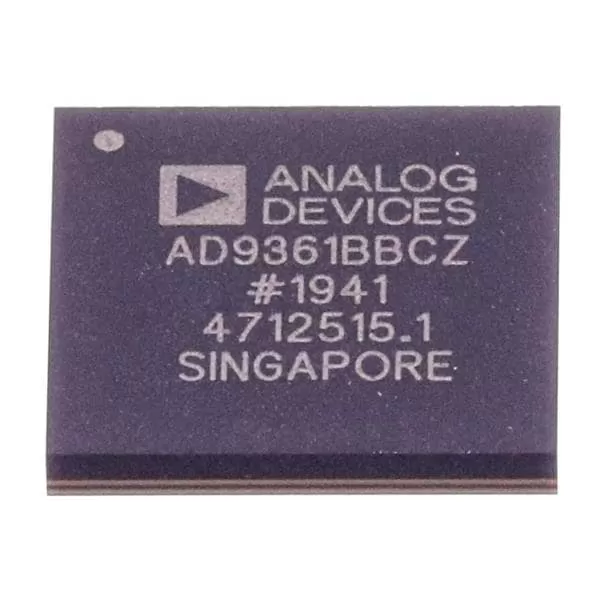

ADG3304BRUZ
Brand: Analog Devices
Analog Devices ADG3304BRUZ is a analog & mixed-signal component designed for Instrumentation and related applications. In stock at Superb Automation — request a quote for competitive pricing and fast delivery.
Product Specifications
ADG3304BRUZ
Analog Devices — Analog & Mixed-Signal ICs
Product Overview
The ADG3304BRUZ from Analog Devices is a high-performance analog / mixed-signal IC providing precision signal acquisition, conversion, and conditioning. Analog Devices (ADI) is a world leader in high-performance analog, mixed-signal, and DSP ICs for instrumentation, healthcare, automotive, and communications.
Superb Automation partners with leading brands including Qorvo, TI, ADI, XILINX, NVIDIA, Intel, ST, MACOM, Renesas, and Coilcraft to provide complete BOM and supply-chain solutions.
Key Features
- High-resolution data conversion with excellent SNR and THD
- Wide dynamic range and high linearity across operating conditions
- Integrated voltage reference with low temperature drift
- Flexible digital interface — SPI, I2C, or parallel options
- Industrial/automotive temperature range with guaranteed specs
- Low power consumption with power-down modes
Key Specifications
| Resolution | bits |
| Channels | — |
| Sample Rate | kSPS |
| Interface | — |
| Supply Voltage | V |
| Operating Temp | °C |
| Package | — |
| INL | LSB |
| SNR | dB |
| THD | dB |
Applications
Precision Instrumentation
Industrial Process Control
Medical Imaging & Diagnostics
Automotive Sensor Interfaces
Communications Infrastructure
Test & Measurement
Request Quote — In Stock, 100% New & Original, Full Warranty
ADG3304BRUZ: four bidirectional level translation channels with no direction pin
The ADG3304BRUZ is not a switch but it sits in the same corner of a board: four bidirectional level translation channels between a low voltage side and a high voltage side, operating from 1.15 V to 5.5 V, with a quiescent current below 5 microamps and no direction pin. The voltage on VCCA sets the logic levels on the A side and VCCY sets the levels on the Y side, and VCCA must always be lower than VCCY.
Published values
| Parameter | Value |
|---|---|
| Channels | four, bidirectional |
| Supply | 1.15 V to 5.5 V |
| Quiescent current | below 5 microamps |
| Direction control | none required |
| Constraint | VCCA must be lower than VCCY |
| Qualification | automotive qualified options |
| Package | TSSOP |
Why the missing direction pin matters
A conventional translator needs a direction pin per channel or per bus, and on a bidirectional bus the processor has to know when to turn the buffer around. That timing is the source of most of the errata in level shifted boards: the turnaround happens one clock too late and the last bit of a read is corrupted. The ADG3304 senses the direction from the signal itself, so the bus turnaround is handled by the part and the firmware does not have to model it.
The price is that the part cannot be used as a general purpose buffer: it is a translator, and it expects to be driving a bus with a defined idle state. On a line that can be driven from both ends at once it will follow whichever side wins, which is why the bus protocol still has to be a proper one.
Quiescent current and the battery arithmetic
Five microamps at 3.3 V is 16.5 microwatts, which is below the self discharge of most small cells. That is the number that lets a translator sit permanently across a battery powered interface without a load switch, and it is why the part appears in portable POS terminals, smart card readers and GPS units.
The current does rise with activity: the part draws charge every time it translates an edge, so a bus that toggles at megahertz rates draws more than the quiescent figure. On a fast SPI link the dynamic current, not the quiescent current, decides the supply budget.
Application notes on the rails
VCCA must be lower than VCCY. This is a hard constraint and not a recommendation: applying VCCA above VCCY puts the internal structures in a state they were not specified for, and the failure appears as a channel that latches on one level. On a board where either rail can come up first, the sequencing has to be checked or the part protected.
The A side logic levels follow VCCA, so a 1.15 V processor can talk to a 3.3 V or 5 V peripheral with no other parts. Below 1.8 V the drive strength and the edge rate both fall, so the trace and the bus capacitance become part of the timing, and a long ribbon cable on the low voltage side will show ringing before the high voltage side does.
Where it fits
SPI and MICROWIRE translation, low voltage ASIC to peripheral interfaces, smart card readers, network switches and storage controllers. It is also the standard fix for an FPGA bank that runs at 1.8 V and a peripheral that only understands 3.3 V.
Buyers usually arrive at one stop BOM sourcing to find the family alternatives, then use vendor consolidation to confirm a substitute before it is fitted; component lead time solutions is the routine for a part that has already stopped shipping.
Two questions buyers ask
Does the ADG3304 need a direction pin? No. It translates in both directions without one, which is its main advantage over a conventional buffer. The bus protocol still has to be one that does not have two drivers active at the same time.
Can the higher voltage side be the lower supply? No. VCCA must always be lower than VCCY. Reversing them puts the part outside its specified operating condition and the fault shows up as a channel that will not release.